- 您現(xiàn)在的位置:買賣IC網(wǎng) > PDF目錄36337 > 935261242112 (NXP SEMICONDUCTORS) SERIAL INPUT LOADING, 20-BIT DAC, PDSO16 PDF資料下載
參數(shù)資料
| 型號: | 935261242112 |
| 廠商: | NXP SEMICONDUCTORS |
| 元件分類: | DAC |
| 英文描述: | SERIAL INPUT LOADING, 20-BIT DAC, PDSO16 |
| 封裝: | 4.40 MM, PLASTIC, SSOP-16 |
| 文件頁數(shù): | 17/21頁 |
| 文件大?。?/td> | 142K |
| 代理商: | 935261242112 |
2000 Jan 10
5
Philips Semiconductors
Preliminary specication
Low-cost stereo lter DAC
UDA1320ATS
7
PINNING
8
FUNCTIONAL DESCRIPTION
8.1
System clock
The UDA1320ATS/N2 operates in slave mode only. This
means in all applications the system devices must provide
the system clock. The system frequency is selectable and
depends on the mode of operation.
The options are 256fs, 384fs and 512fs for the L3 mode
and 256fs plus 384fs for the static mode. The system clock
must be locked in frequency to the digital interface input
signals.
The UDA1320ATS/N2 supports sampling frequencies
from 16kHz up to 48kHz
8.2
Application modes
The application mode can be set with the tri-value
APPSEL pin, to L3 mode (APPSEL = VSSD) or to either of
two static modes (APPSEL = 0.5VDDD or
APPSEL = VDDD). See Table 1 for APPL0 to APPL3 pin
functions (active = HIGH).
Table 1
Selection modes via APPSEL (note 1)
For example, in static pin control mode, the output signal
can be soft muted by setting APPL0 HIGH. De-emphasis
can be switched on for 44.1 kHz by setting APPL1 HIGH.
APPL1 LOW will disable de-emphasis.
Note that when L3 interface is used, an L3 initialisation
must be done when the IC is powered up!
In L3 mode pin APPL0 must be set to LOW.
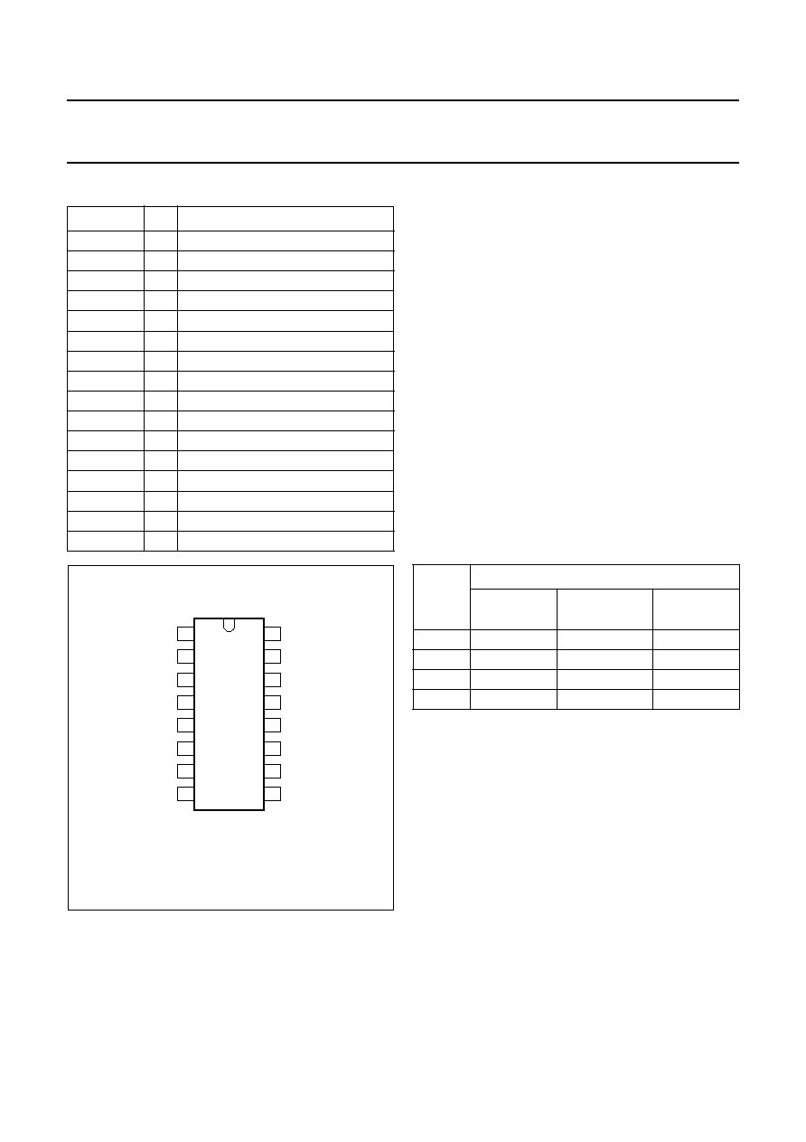
SYMBOL
PIN
DESCRIPTION
BCK
1
bit clock
WS
2
word select
DATAI
3
data input
VDDD
4
digital power supply
VSSD
5
digital ground
SYSCLK
6
system clock: 256fs, 384fs, 512fs
APPSEL
7
application mode select
APPL3
8
application pin 3
APPL2
9
application pin 2
APPL1
10
application pin 1
APPL0
11
application pin 0
VREF(DAC)
12
DAC reference voltage
VDDA
13
analog supply voltage
VO(L)
14
left output voltage
VSSA
15
analog ground
VO(R)
16
right output voltage
Fig.2 Pin configuration.
handbook, halfpage
UDA1320A
MGM817
1
2
3
4
5
6
7
8
16
15
14
13
12
11
10
9
VO(R)
BCK
VSSA
WS
VO(L)
DATAI
VDDA
VDDD
VREF(DAC)
VSSD
APPL0
SYSCLK
APPL1
APPSEL
APPL2
APPL3
PIN
APPSEL
VSSD
0.5VDDD
(384fs)
VDDD
(256fs)
APPL0
TEST
MUTE
APPL1
L3CLOCK
DEEM
APPL2
L3MODE
SF0
APPL3
L3DATA
SF1
相關(guān)PDF資料 |
PDF描述 |
|---|---|
| 935261315112 | 2 CHANNEL(S), VOLUME CONTROL CIRCUIT, PDSO20 |
| 935261315118 | 2 CHANNEL(S), VOLUME CONTROL CIRCUIT, PDSO20 |
| 935261316112 | 2 CHANNEL(S), VOLUME CONTROL CIRCUIT, PDSO20 |
| 935261316118 | 2 CHANNEL(S), VOLUME CONTROL CIRCUIT, PDSO20 |
| 935261327518 | DUAL 1-CH 8-BIT PROPRIETARY METHOD ADC, PARALLEL ACCESS, PQFP64 |
相關(guān)代理商/技術(shù)參數(shù) |
參數(shù)描述 |
|---|---|
| 935262025112 | 制造商:NXP Semiconductors 功能描述:SUB ONLY IC |
| 935262217118 | 制造商:NXP Semiconductors 功能描述:Real Time Clock Serial 8-Pin SO T/R |
| 935264217557 | 制造商:NXP Semiconductors 功能描述:SUB ONLY IC |
| 935267356112 | 制造商:NXP Semiconductors 功能描述:IC TEA1507PN |
| 935268081112 | 制造商:NXP Semiconductors 功能描述:SUB ONLY IC |
發(fā)布緊急采購,3分鐘左右您將得到回復(fù)。