- 您現(xiàn)在的位置:買賣IC網(wǎng) > PDF目錄298557 > 7P512CFA4500C25 (WHITE ELECTRONIC DESIGNS CORP) 256M X 16 FLASH 3V PROM CARD, 250 ns, XMA50 PDF資料下載
參數(shù)資料
| 型號(hào): | 7P512CFA4500C25 |
| 廠商: | WHITE ELECTRONIC DESIGNS CORP |
| 元件分類: | PROM |
| 英文描述: | 256M X 16 FLASH 3V PROM CARD, 250 ns, XMA50 |
| 封裝: | CARD-50 |
| 文件頁數(shù): | 28/32頁 |
| 文件大小: | 264K |
| 代理商: | 7P512CFA4500C25 |
第1頁第2頁第3頁第4頁第5頁第6頁第7頁第8頁第9頁第10頁第11頁第12頁第13頁第14頁第15頁第16頁第17頁第18頁第19頁第20頁第21頁第22頁第23頁第24頁第25頁第26頁第27頁當(dāng)前第28頁第29頁第30頁第31頁第32頁

5
White Electronic Designs Corporation (508) 485-4000 www.whiteedc.com
White Electronic Designs
CompactFlashTM Cards
CFA45 Series
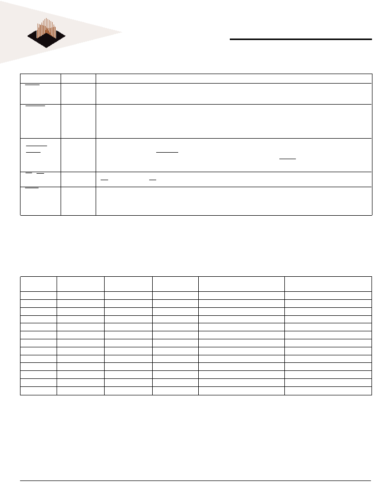
Symbol
Type
Name and Function
WAIT, IORDY OUTPUT
WAIT: This signal outputs low level for the purpose of delaying memory access cycle or I/O access cycle. In
True IDE Mode this output signal may be used as IORDY. As for this controller, this output is high impedance
state constantly.
INPACK
OUTPUT
INPUT ACKNOWLEDGE: This signal is not used in the memory card mode. The Input acknowledge signal is
asserted by the CF Card when the card is selected and responding to an I/O read cycle at the address that is
on the address bus. This signal is used by the host to control the enable of any input data buffers between the
CF Card and the CPU. In True IDE mode, this output signal is not used and should be connected to VCC at
the host.
BVD1,
INPUT/
BATTERY VOLTAGE DETECTION, STATUS CHANGE, PASS DIAGNOSTIC: In the memory card mode, BVD1
STSCHG,
OUTPUT
outputs the battery voltage status in the card. This card has no battery, so this output is high level constantly.
PDIAG
In the I/O card mode, STSCHG is used for changing the status of the Configuration status register in the
Attribute area, while the card is set I/O card interface. In True IDE Mode, PDIAG is the Pass Diagnostic signal
in the Master/Slave handshake protocol.
VS1, VS2
OUTPUT
VCC VOLTAGE SENSE: These signals are intended to notify the socket of the CF Cards CIS VCC requirement.
VS1 is held low and VS2 is not connected in this card.
CSEL
INPUT
CARD SELECT: This signal is not used in the memory card mode and I/O card mode. This internally pulled up
signal is used to configure this device as a Master or a Slave when configured in the True IDE Mode. When
this pin is grounded, this device is configured as a Master. When the pin is open, this device is configured as
a Slave.
INTERFACE SIGNALS DESCRIPTION CONT.
COMPACTFLASHTM/PCMCIA-ATA REGISTER MAPPING ADDRESS.
COMPACTFLASHTM/PCMCIA-ATA I/O MAPPING ADDRESS
REG
Primary I/O
Secondary I/O
Independent I/O
IORD = L
IOWR = L
A[10:0]
A[3:0]
L
1F0H
170H
0H
Read Even Data
Write Even Data
L
1F1H
171H
1H
Error Register
Feature Register
L
1F2H
172H
2H
Sector Count
L
1F3H
173H
3H
Sector Number
L
1F4H
174H
4H
Cylinder Low
L
1F5H
175H
5H
Cylinder High
L
1F6H
176H
6H
Drive/Head
L
1F7H
177H
7H
Status Register
Command
L
-
8H
Duplicate Read Even Data
Duplicate Write Even Data
L
-
9H
Duplicate Read Odd Data
Duplicate Write Odd Data
L
-
0DH
Duplicate Error
Duplicate Feature
L
3F6H
376H
0EH
Alternate Status
Device Control
L
3F7H
377H
0FH
Drive Address
Reserved
相關(guān)PDF資料 |
PDF描述 |
|---|---|
| 7T5101 | Logic IC |
| 7T5125 | Logic IC |
| 7T5151 | Logic IC |
| 7T5175 | Logic IC |
| 7T5200 | Logic IC |
相關(guān)代理商/技術(shù)參數(shù) |
參數(shù)描述 |
|---|---|
| 7P601V330K042 | 制造商:CDE 制造商全稱:Cornell Dubilier Electronics 功能描述:Type 7P 55 ∑C Photoflash, High-Energy, Long Life, Aluminum |
| 7P601V360A032 | 功能描述:鋁質(zhì)電解電容器-管理單元 600uF 360V PHOTO RoHS:否 制造商:Nichicon 電容:470 uF 容差:20 % 電壓額定值:450 V ESR: 工作溫度范圍:- 25 C to + 105 C 系列:AR 直徑:35 mm 長度:45 mm 引線間隔:10 mm 產(chǎn)品:General Purpose Electrolytic Capacitors |
| 7P701V330A042 | 制造商:CDE 制造商全稱:Cornell Dubilier Electronics 功能描述:Type 7P 55 ∑C Photoflash, High-Energy, Long Life, Aluminum |
| 7P701V360A042 | 制造商:CDE 制造商全稱:Cornell Dubilier Electronics 功能描述:Type 7P 55 ∑C Photoflash, High-Energy, Long Life, Aluminum |
| 7P801V330A042 | 制造商:未知廠家 制造商全稱:未知廠家 功能描述:Photoflash, High-Energy, Long Life, Aluminum |
發(fā)布緊急采購,3分鐘左右您將得到回復(fù)。