- 您現(xiàn)在的位置:買(mǎi)賣(mài)IC網(wǎng) > PDF目錄360445 > 74F8963 (NXP Semiconductors N.V.) 9-Bit latched bidirectional Futurebus transceivers open-collector PDF資料下載
參數(shù)資料
| 型號(hào): | 74F8963 |
| 廠商: | NXP Semiconductors N.V. |
| 英文描述: | 9-Bit latched bidirectional Futurebus transceivers open-collector |
| 中文描述: | 9位鎖存雙向Futurebus收發(fā)器集電極開(kāi)路 |
| 文件頁(yè)數(shù): | 10/10頁(yè) |
| 文件大小: | 97K |
| 代理商: | 74F8963 |
Philips Semiconductors FAST Products
Product specification
74F8962/8963
9-Bit latched bidirectional Futurebus transceivers
(open-collector)
March 11, 1993
10
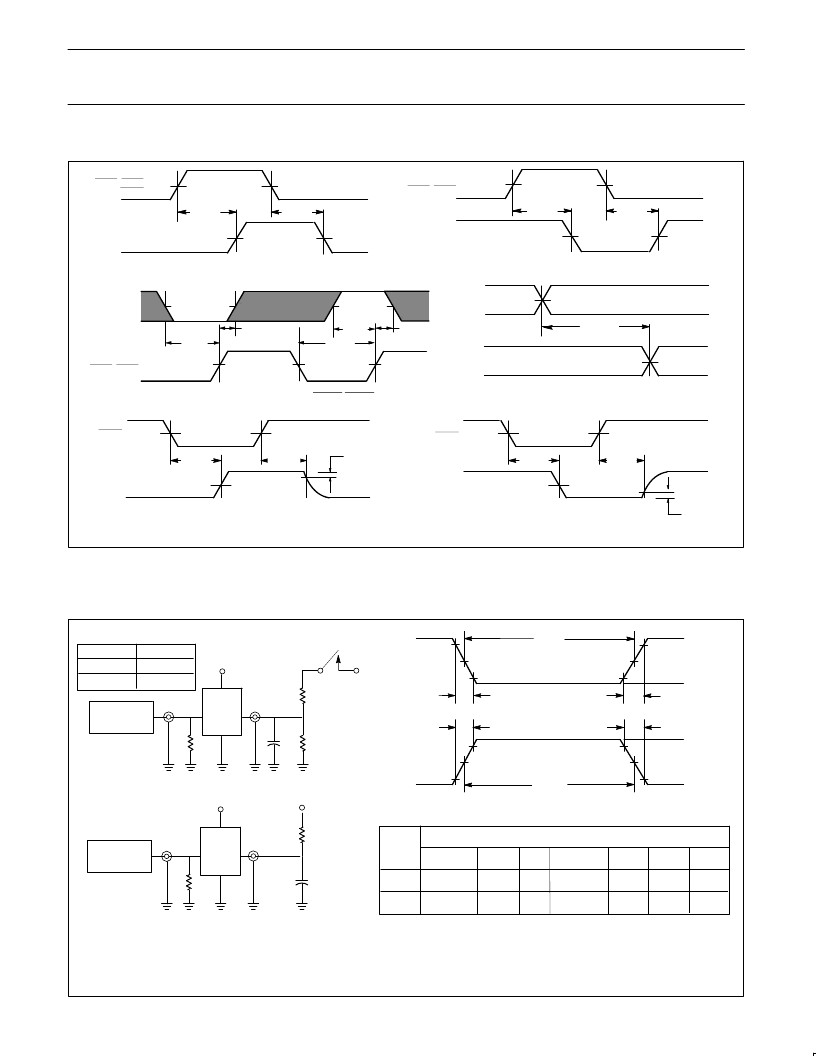
AC WAVEFORMS
V
M
V
M
V
M
V
M
Waveform 1. Propagation delay for data or output enable or
latch enable to output
Waveform 3. Data setup and hold times and LEAB/LEBA pulse widths
Waveform 5. 3–state output enable time to high level
and output disable time from high level
Waveform 6. 3-state output enable time to low level
and output disable time from low level
V
M
V
M
V
M
V
M
V
M
V
M
t
su
(L)
t
su
(H)
t
h
(L)
t
h
(H)
V
M
V
M
V
M
t
PHZ
t
PZH
V
OH
-0.3V
0V
V
M
V
M
V
M
t
PLZ
t
PZL
V
OL
+0.3V
An
OEAB
An
AOn, Bn
AIn, Bn,
LEAB, LEBA
OEAB
t
PLH
t
PHL
V
M
t
w
(L)
V
M
V
M
V
M
V
M
Waveform 2. Propagation delay for data or latch enable to
output
An, Bn
t
PHL
t
PLH
AIn, Bn,
LEAB, LEBA
AIn, Bn
LEAB, LEBA
OEAB
Waveform 4. Output skew
V
M
V
M
t
sk(o)
AOn, Bn
AOn, Bn
NOTES TO AC WAVEFORMS
1. For all waveforms, V
M
= 1.5V.
2. The shaded areas indicate when the input is permitted to change for predictable output performance.
TEST CIRCUITS AND WAVEFORMS
t
w
90%
V
M
10%
90%
V
M
10%
90%
V
M
10%
90%
V
M
10%
NEGATIVE
PULSE
POSITIVE
PULSE
t
w
AMP (V)
Low V
Low V
t
THL (
t
f
)
INPUT PULSE REQUIREMENTS
rep. rate
t
w
t
TLH
t
THL
Input pulse definition
V
CC
family
74F
D.U.T.
PULSE
GENERATOR
R
L
C
L
R
T
V
IN
V
OUT
Test circuit for 3–state outputs on A port
DEFINITIONS:
R
L
=
C
L
=
R
U
=
C
D
=
R
T
=
Load resistor; see AC electrical characteristics for value.
Load capacitance includes jig and probe capacitance; see AC electrical characteristics for value.
Pull up resistor; see AC electrical characteristics for value.
Load capacitance includes jig and probe capacitance; see AC electrical characteristics for value.
Termination resistance should be equal to Z
OUT
of pulse generators.
t
THL (
t
f
)
t
TLH (
t
r
)
t
TLH (
t
r
)
AMP (V)
amplitude
V
M
R
L
7.0V
V
CC
D.U.T.
PULSE
GENERATOR
C
D
R
T
V
IN
V
OUT
Test circuit for outputs on B port
R
U
7.0V
Low V
SWITCH POSITION
TEST
t
PLZ
, t
PZL
SWITCH
closed
open
All other
A port
3.0V
0.0V
1.5V
1MHz
500ns
2.5ns
2.5ns
B port
3.0V
1.0V
1.5V
1MHz
500ns
4.0ns
4.0ns
相關(guān)PDF資料 |
PDF描述 |
|---|---|
| 74F8965 | 9-Bit address/data Futurebus transceiver, ADT |
| 74F8966 | 9-Bit address/data Futurebus transceiver, ADT |
| 74F978PC | Octal D-Type Flip-Flop |
| 74F978QC | Octal D-Type Flip-Flop |
| 74F978SC | Octal D-Type Flip-Flop |
相關(guān)代理商/技術(shù)參數(shù) |
參數(shù)描述 |
|---|---|
| 74F8965 | 制造商:PHILIPS 制造商全稱(chēng):NXP Semiconductors 功能描述:9-Bit address/data Futurebus transceiver, ADT |
| 74F8966 | 制造商:PHILIPS 制造商全稱(chēng):NXP Semiconductors 功能描述:9-Bit address/data Futurebus transceiver, ADT |
| 74F899 | 制造商:FAIRCHILD 制造商全稱(chēng):Fairchild Semiconductor 功能描述:9-Bit Latchable Transceiver with Parity Generator/Checker |
| 74F899_YCB3026T WAF | 制造商:Fairchild Semiconductor Corporation 功能描述: |
| 74F899_YCC3026B WAF | 制造商:Fairchild Semiconductor Corporation 功能描述: |
發(fā)布緊急采購(gòu),3分鐘左右您將得到回復(fù)。