- 您現(xiàn)在的位置:買賣IC網(wǎng) > PDF目錄360230 > 522923D Dual/Triple Ultra-Low-Voltage SOT23 µP Supervisory Circuits PDF資料下載
參數(shù)資料
| 型號(hào): | 522923D |
| 英文描述: | Dual/Triple Ultra-Low-Voltage SOT23 µP Supervisory Circuits |
| 中文描述: | 集成電路 |
| 文件頁(yè)數(shù): | 16/24頁(yè) |
| 文件大小: | 418K |
| 代理商: | 522923D |
第1頁(yè)第2頁(yè)第3頁(yè)第4頁(yè)第5頁(yè)第6頁(yè)第7頁(yè)第8頁(yè)第9頁(yè)第10頁(yè)第11頁(yè)第12頁(yè)第13頁(yè)第14頁(yè)第15頁(yè)當(dāng)前第16頁(yè)第17頁(yè)第18頁(yè)第19頁(yè)第20頁(yè)第21頁(yè)第22頁(yè)第23頁(yè)第24頁(yè)
16
LTC1286/LTC1298
APPLICATIO
I
FOR
ATIO
U
Differential Inputs
With differential inputs, the ADC no longer converts just a
single voltage but rather the difference between two volt-
ages. In this case, the voltage on the selected “+” input is
still sampled and held and therefore may be rapidly time
varying just as in single-ended mode. However, the volt-
age on the selected “–” input must remain constant and be
free of noise and ripple throughout the conversion time.
Otherwise, the differencing operation may not be per-
formed accurately. The conversion time is 12 CLK cycles.
Therefore, a change in the “–” input voltage during this
interval can cause conversion errors. For a sinusoidal
voltage on the “–” input this error would be:
V
ERROR (MAX)
= V
PEAK
×
2
×
π
×
f(“–”)
×
12/f
CLK
Where f(“–”) is the frequency of the “–” input voltage,
V
PEAK
is its peak amplitude and f
CLK
is the frequency of the
CLK. In most cases V
ERROR
will not be significant. For a
60Hz signal on the “–” input to generate a 1/4LSB error
(305
μ
V) with the converter running at CLK = 200kHz, its
peak value would have to be 13.48mV.
W
U
U
ANALOG INPUTS
Because of the capacitive redistribution A/D conversion
techniques used, the analog inputs of the LTC1286/
LTC1298 have capacitive switching input current spikes.
These current spikes settle quickly and do not cause a
problem. However, if large source resistances are used or
if slow settling op amps drive the inputs, care must be
taken to insure that the transients caused by the current
spikes settle completely before the conversion begins.
“+” Input Settling
The input capacitor of the LTC1286 is switched onto “+”
input during the t
SMPL
time (see Figure 1) and samples the
input signal within that time. However, the input capacitor
of the LTC1298 is switched onto “+” input during the
sample phase (t
SMPL
, see Figure 7). The sample phase is
1 1/2 CLK cycles before conversion starts. The voltage on
the “+” input must settle completely within t
SMPLE
for the
LTC1286 and the LTC1298 respectively. Minimizing
R
SOURCE+
and C1 will improve the input settling time. If a
large “+” input source resistance must be used, the
sample time can be increased by using a slower CLK
frequency.
“–” Input Settling
At the end of the t
SMPL
, the input capacitor switches to the
“–” input and conversion starts (see Figures 1 and 7).
During the conversion, the “+” input voltage is effectively
“held” by the sample-and-hold and will not affect the
conversion result. However, it is critical that the “–” input
voltage settles completely during the first CLK cycle of the
conversion time and be free of noise. Minimizing R
SOURCE–
and C2 will improve settling time. If a large “–” input
source resistance must be used, the time allowed for
settling can be extended by using a slower CLK frequency.
Input Op Amps
When driving the analog inputs with an op amp it is
important that the op amp settle within the allowed time
(see Figure 7). Again, the“+” and “–” input sampling times
can be extended as described above to accommodate
slower op amps. Most op amps, including the LT1006 and
LT1413 single supply op amps, can be made to settle well
even with the minimum settling windows of 6
μ
s (“+”
input) which occur at the maximum clock rate of 200kHz.
Source Resistance
The analog inputs of the LTC1286/LTC1298 look like a
20pF capacitor (C
IN
) in series with a 500
resistor (R
ON
)
as shown in Figure 8. C
IN
gets switched between the
selected “+” and “–” inputs once during each conversion
cycle. Large external source resistors and capacitances
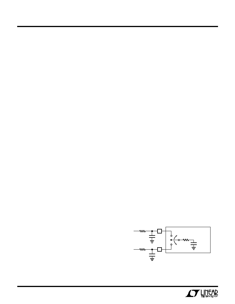
Figure 8. Analog Input Equivalent Circuit
R
ON
= 500
C
IN
= 20pF
LTC1286/98
“+”
INPUT
R
SOURCE
+
V
IN
+
C1
“–”
INPUT
R
SOURCE
–
V
IN
–
C2
LTC1286/98 F08
相關(guān)PDF資料 |
PDF描述 |
|---|---|
| 522929C | IC |
| 522946A | Dual/Triple Ultra-Low-Voltage SOT23 µP Supervisory Circuits |
| 522925X | IC |
| 52602499 | LOETSTATION WECP 82 |
| 52610-1090 | Dual/Triple Ultra-Low-Voltage SOT23 µP Supervisory Circuits |
相關(guān)代理商/技術(shù)參數(shù) |
參數(shù)描述 |
|---|---|
| 5229-24CPB | 制造商:MOLEX 制造商全稱:Molex Electronics Ltd. 功能描述:2.54mm (.100) Vertical, Non-ZIF, Low Profile Receptacle, 24 Circuits |
| 522925-000 | 制造商:TE Connectivity 功能描述:Shrink Boot Adapters 180° 制造商:TE Connectivity 功能描述:TXR40AB00-2012CI - Bulk |
| 5229-25APB | 制造商:MOLEX 制造商全稱:Molex Electronics Ltd. 功能描述:2.54mm (.100) Right Angle, Non-ZIF, Low Profile Receptacle, 25 Circuits |
| 5229-25CPB | 制造商:MOLEX 制造商全稱:Molex Electronics Ltd. 功能描述:2.54mm (.100) Vertical, Non-ZIF, Low Profile Receptacle, 25 Circuits |
| 522925X | 制造商:未知廠家 制造商全稱:未知廠家 功能描述:IC |
發(fā)布緊急采購(gòu),3分鐘左右您將得到回復(fù)。