- 您現(xiàn)在的位置:買賣IC網(wǎng) > PDF目錄384068 > μPD98408 (NEC Corp.) ATM Physical Interface(ATM 物理接口) PDF資料下載
參數(shù)資料
| 型號(hào): | μPD98408 |
| 廠商: | NEC Corp. |
| 英文描述: | ATM Physical Interface(ATM 物理接口) |
| 中文描述: | ATM物理接口(自動(dòng)柜員機(jī)物理接口) |
| 文件頁數(shù): | 14/32頁 |
| 文件大?。?/td> | 193K |
| 代理商: | ΜPD98408 |
第1頁第2頁第3頁第4頁第5頁第6頁第7頁第8頁第9頁第10頁第11頁第12頁第13頁當(dāng)前第14頁第15頁第16頁第17頁第18頁第19頁第20頁第21頁第22頁第23頁第24頁第25頁第26頁第27頁第28頁第29頁第30頁第31頁第32頁
14
μ
PD98408
(3/3)
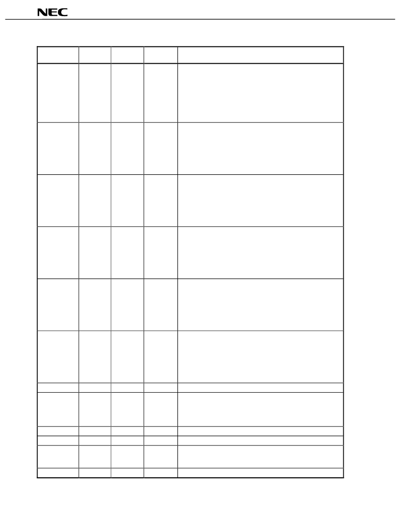
Pin Name
Pin No.
I/O
Active
Level
Function
IC/RDATA5
42
O
/
Two pin functions can be selected according to the level of the
PMDONLY pin.
When PMDONLY = 0 (IC):
No signal should be connected to this pin.
When PMDONLY = 1 (RDATA5):
Output pin for the data received from the PMD receiver
(Circuit 5).
IC/TDATA1
45
I
(with pull-
down
resistor)
/
Two pin functions can be selected according to the level of the
PMDONLY pin.
When PMDONLY = 0 (IC):
No signal should be connected to this pin.
When PMDONLY = 1 (TDATA1):
Input pin for transmit data for the PMD transmitter (Circuit 1).
IC/TDATA2
46
I
(with pull-
down
resistor)
/
Two pin functions can be selected according to the level of the
PMDONLY pin.
When PMDONLY = 0 (IC):
No signal should be connected to this pin.
When PMDONLY = 1 (TDATA2):
Input pin for transmit data for the PMD transmitter (Circuit 2).
IC/TDATA3
48
I
(with pull-
down
resistor)
/
Two pin functions can be selected according to the level of the
PMDONLY pin.
When PMDONLY = 0 (IC):
No signal should be connected to this pin.
When PMDONLY = 1 (TDATA3):
Input pin for transmit data for the PMD transmitter (Circuit 3).
IC/TDATA4
49
I
(with pull-
down
resistor)
/
Two pin functions can be selected according to the level of the
PMDONLY pin.
When PMDONLY = 0 (IC):
No signal should be connected to this pin.
When PMDONLY = 1 (TDATA4):
Input pin for transmit data for the PMD transmitter (Circuit 4).
SIN/TDATA5
50
I
(with pull-
down
resistor)
H/
Two pin functions can be selected according to the level of the
PMDONLY pin.
When PMDONLY = 0 (SIN):
X_8 command transmit timing signal input pin.
When PMDONLY = 1 (TDATA5):
Input pin for transmit data for the PMD transmitter (Circuit 5).
SOUT
54
O
H
X_8 command receive timing signal output pin.
PMDONLY
18
I
(with pull-
down
resistor)
Specifies the mode of the
μ
PD98408: whether it is operated as
PMD + TC or as PMD only.
0:
Operation as PMD + TC.
1:
Operation as PMD only.
TCLOCK
57
I
Transmit clock (32 MHz) input pin
RESET_B
55
I
L
Input pin for the reset signal for the entire
μ
PD98408.
IC
5, 6, 14,
15, 85,
144, 145
No signal should be connected to these pins.
CG
113
I
Should be connected to GND for normal use.
相關(guān)PDF資料 |
PDF描述 |
|---|---|
| μPD98411 | Ultraframer DS3/E3/DS2/E2/DS1/E1/DS0 |
| μPD98501 | Network Controller(網(wǎng)絡(luò)控制器) |
| μPG103B | Wide-Band Amplifier(寬帶放大器) |
| μPG110B | 2 to 8 GHz WIDE BAND AMPLIFIER(2-8GHz 寬帶放大器) |
| μPG132G | L-Band SPDT Switch(長(zhǎng)波段單刀雙擲開關(guān)) |
相關(guān)代理商/技術(shù)參數(shù) |
參數(shù)描述 |
|---|---|
| PD98CNT30QMU | 制造商:Carlo Gavazzi 功能描述:PHOTO TS PL 30M AC/DC NO+NC |
| PD9909-59 | 制造商:Philco/Philips 功能描述: |
| PD9930-51 | 制造商:Philco/Philips 功能描述: |
| PD9933-59 | 制造商:Philco/Philips 功能描述: |
| PD9941-59 | 制造商:Philco/Philips 功能描述: |
發(fā)布緊急采購,3分鐘左右您將得到回復(fù)。