- 您現(xiàn)在的位置:買(mǎi)賣(mài)IC網(wǎng) > PDF目錄9084 > XRT71D00IQTR-F (Exar Corporation)IC JITTER ATTENUATOR SGL 32TQFP PDF資料下載
參數(shù)資料
| 型號(hào): | XRT71D00IQTR-F |
| 廠(chǎng)商: | Exar Corporation |
| 文件頁(yè)數(shù): | 15/26頁(yè) |
| 文件大小: | 0K |
| 描述: | IC JITTER ATTENUATOR SGL 32TQFP |
| 標(biāo)準(zhǔn)包裝: | 1,500 |
| 類(lèi)型: | * |
| PLL: | 是 |
| 輸入: | 時(shí)鐘 |
| 輸出: | 時(shí)鐘 |
| 電路數(shù): | 1 |
| 比率 - 輸入:輸出: | 3:2 |
| 差分 - 輸入:輸出: | 無(wú)/無(wú) |
| 頻率 - 最大: | 44.736MHz |
| 除法器/乘法器: | 無(wú)/無(wú) |
| 電源電壓: | 3.135 V ~ 5.25 V |
| 工作溫度: | -40°C ~ 85°C |
| 安裝類(lèi)型: | 表面貼裝 |
| 封裝/外殼: | 32-LQFP |
| 供應(yīng)商設(shè)備封裝: | 32-TQFP(7x7) |
| 包裝: | 帶卷 (TR) |
第1頁(yè)第2頁(yè)第3頁(yè)第4頁(yè)第5頁(yè)第6頁(yè)第7頁(yè)第8頁(yè)第9頁(yè)第10頁(yè)第11頁(yè)第12頁(yè)第13頁(yè)第14頁(yè)當(dāng)前第15頁(yè)第16頁(yè)第17頁(yè)第18頁(yè)第19頁(yè)第20頁(yè)第21頁(yè)第22頁(yè)第23頁(yè)第24頁(yè)第25頁(yè)第26頁(yè)
XRT71D00
á
E3/DS3/STS-1 JITTER ATTENUATOR
REV. 1.2.0
21
2.0
OPERATING MODE
2.1
HARDWARE MODE
The HOST/HW pin (pin 12) is used to select the oper-
ating mode of the XRT71D00. In Hardware mode
(connect this pin to ground), the serial processor in-
terface is disabled and hardwired pins are used to
control configuration and report status.
2.1.1
Host Mode:
In Host mode ( connect the HOST/HW pin to VDD),
the serial port interface pins are used to control con-
figuration and status report. In this mode, serial inter-
face pins : SDI, SDO, SClk and CS are used.
A listing of these Command Registers, their Address-
es, and their bit-formats are listed below in Table 6.
3.0
MICROPROCESSOR SERIAL INTERFACE
The serial interface for the XRT71D00 and XRT73L00
E3/DS3/STS-1 LIU are the same, which makes it
easy to configure both the XRT71D00 and the LIU
with a single CS, SDI, SDO and SClk input and out-
put pins.
3.1
SERIAL INTERFACE OPERATION.
Serial interface data structure and timings are provid-
The clock signal is provided to the SClk and the CS is
asserted for 50 ns prior to the first rising edge of the
SClk.
3.1.1
Bit Descriptions
3.1.1.1
Bit 1—“R/W” (Read/Write) Bit
This bit will be clocked into the SDI input, on the first
rising edge of SClk (after CS has been asserted).
This bit indicates whether the current operation is a
“Read” or “Write” operation. A “1” in this bit specifies
a “Read” operation, a “0” in this bit specifies a “Write”
operation.
3.1.1.2
Bits 2 through 6
The five (5) bit Address Values (labeled A0, A1, A2
,A3, and A4)
The next four rising edges of the SClk signal will clock
in the 5-bit address value for this particular Read (or
Write) operation. The address selects the Command
Register for reading data from, or writing data to. The
address bits to the SDI input pin is applied in ascend-
ing order with the LSB (least significant bit) first.
Bit 7---A5
A5 must be set to “0”, as shown in Figure 11.
Bit 8—A6
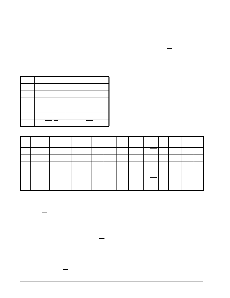
TABLE 5: HARDWARE MODE PIN FUNCTIONS
PIN #PIN NAME
HARDWARE MODE FUNCTION
10
ClkES/(SDI)
ClkES
11
FSS/(SClk)
FSS
15
BWS/Ch_Addr_1
BWS
18
DJA/(SDO)
DJA
28
Ch_Addr_0
None
29
E3/DS3/(CS)E3/DS3
TABLE 6: ADDRESS AND BIT FORMATS OF THE COMMAND REGISTERS
ADDR
COMMAND
REGISTER
CH_ADDR_1 CH_ADDR_0
TYPE
D7
D6
D5
D4
D3
D2
D1
D0
0X06
CR6
0
R/W
***
STS-1
E3/DS3
DJA
BWS
ClkES FSS
0x07
CR7
0
RO
***
FL
0x0E
CR14
0
1
R/W
***
STS-1
E3/DS3
DJA
BWS
ClkES FSS
0x0F
CR15
0
1
RO
***
FL
0x16
CR22
1
0
R/W
***
STS-1
E3/DS3
DJA
BWS
ClkES FSS
0x17
CR22
1
0
RO
***
FL
相關(guān)PDF資料 |
PDF描述 |
|---|---|
| X9421WV14I-2.7T1 | IC XDCP SGL 64-TAP 10K 14-TSSOP |
| X9421WV14-2.7T1 | IC XDCP SGL 64-TAP 10K 14-TSSOP |
| SY89536LHZ | IC SYNTHESIZR LVPECL/HSTL 64TQFP |
| VI-253-MW-S | CONVERTER MOD DC/DC 24V 100W |
| V28A5H175B | CONVERTER MOD DC/DC 5V 175W |
相關(guān)代理商/技術(shù)參數(shù) |
參數(shù)描述 |
|---|---|
| XRT71D03 | 制造商:EXAR 制造商全稱(chēng):EXAR 功能描述:3 CHANNEL E3/DS3/STS-1 JITTER ATTENUATOR |
| XRT71D03ES | 功能描述:時(shí)鐘合成器/抖動(dòng)清除器 3CH T3/E3JA w/T73LC03A RoHS:否 制造商:Skyworks Solutions, Inc. 輸出端數(shù)量: 輸出電平: 最大輸出頻率: 輸入電平: 最大輸入頻率:6.1 GHz 電源電壓-最大:3.3 V 電源電壓-最小:2.7 V 封裝 / 箱體:TSSOP-28 封裝:Reel |
| XRT71D03IV | 制造商:EXAR 制造商全稱(chēng):EXAR 功能描述:3 CHANNEL E3/DS3/STS-1 JITTER ATTENUATOR |
| XRT71D03IV-F | 功能描述:時(shí)鐘合成器/抖動(dòng)清除器 RoHS:否 制造商:Skyworks Solutions, Inc. 輸出端數(shù)量: 輸出電平: 最大輸出頻率: 輸入電平: 最大輸入頻率:6.1 GHz 電源電壓-最大:3.3 V 電源電壓-最小:2.7 V 封裝 / 箱體:TSSOP-28 封裝:Reel |
| XRT71D03IVTR-F | 功能描述:時(shí)鐘合成器/抖動(dòng)清除器 RoHS:否 制造商:Skyworks Solutions, Inc. 輸出端數(shù)量: 輸出電平: 最大輸出頻率: 輸入電平: 最大輸入頻率:6.1 GHz 電源電壓-最大:3.3 V 電源電壓-最小:2.7 V 封裝 / 箱體:TSSOP-28 封裝:Reel |
發(fā)布緊急采購(gòu),3分鐘左右您將得到回復(fù)。