- 您現在的位置:買賣IC網 > PDF目錄1974 > XPC8240RZU250E (Freescale Semiconductor)MCU HOST PROCESSOR 352-TBGA PDF資料下載
參數資料
| 型號: | XPC8240RZU250E |
| 廠商: | Freescale Semiconductor |
| 文件頁數: | 5/8頁 |
| 文件大?。?/td> | 0K |
| 描述: | MCU HOST PROCESSOR 352-TBGA |
| 標準包裝: | 24 |
| 系列: | MPC82xx |
| 處理器類型: | 32-位 MPC82xx PowerQUICC II |
| 速度: | 200MHz |
| 電壓: | 2.5V |
| 安裝類型: | 表面貼裝 |
| 封裝/外殼: | 352-LBGA |
| 供應商設備封裝: | 352-TBGA(35x35) |
| 包裝: | 托盤 |
MPC8240 Part Number Specification for the XPC8240RXXnnnx Series
5
Ordering Information
Notes:
1. The processor HID1 values only represent the multiplier of the processor’s PLL (memory-to-processor multiplier);
thus, multiple MPC8240 PLL_CFG[0:4] values may have the same processor HID1 value. This implies that system
software cannot read the HID1 register and associate it with a unique PLL_CFG[0:4] value.
2. PLL_CFG[0:4] settings not listed (00110, 01001, 01011, 01101, 01111, 10001, 10011, 10101, 10111, 11001, and
11011) are reserved.
3. In PLL bypass mode, the PCI_SYNC_IN input signal clocks the internal processor directly, the peripheral logic PLL
is disabled, and the bus mode is set for 1:1 (PCI:Mem) mode operation. This mode is intended for hardware modeling
support. The AC timing specifications given in this document do not apply in PLL bypass mode.
4. In clock-off mode, no clocking occurs inside the MPC8240 regardless of the PCI_SYNC_IN input.
5. Limited due to maximum memory VCO = 225 MHz.
6. Limited due to minimum CPU VCO = 200 MHz.
7. Limited due to minimum memory VCO = 100 MHz.
8. For clarity, range values are shown rounded down to the nearest whole number (decimal place accuracy removed).
9. Note that the 250-MHz part is available only in the XPC8240RZUnnnx number series.
1.9
Ordering Information
Ordering information for the parts fully covered by this specification document is provided in Section 1.9.1,
5
00101
00110
Bypass
2.5 (5)
7
00111
11000
Bypass
3 (6)
8
01000
11000
33 6–56 5
33–56
100–168
1 (4)
3 (6)
A
01010
00111
25–27
50–55
225–250
2 (4)
4.5 (9)
C
01100
00110
25–50
50–100
125–250
2 (4)
2.5 (5)
E
01110
11000
25–41
50–83
150–250
2 (4)
3 (6)
10
10000
00100
25–33
75–100
150–200
3 (6)
2 (4)
12
10010
00100
33–66
50–100
100–200
1.5 (3)
2 (4)
14
10100
11110
25–35
50–71
175–250
2 (4)
3.5 (7)
16
10110
11010
25–31
50–62
200–250
2 (4)
4 (8)
18
11000
25–33
62–83
186–250
2.5 (5)
3 (6)
1A
11010
50 7–62
50–62
200–250
1 (2)
4 (8)
1C
11100
11000
33 7–55
50–83
150–250
1.5 (3)
3 (6)
1D
11101
00110
33 7–66
50–100
125–250
1.5 (3)
2.5 (5)
1E
11110
01111
Not usable
Off
1F
11111
Off
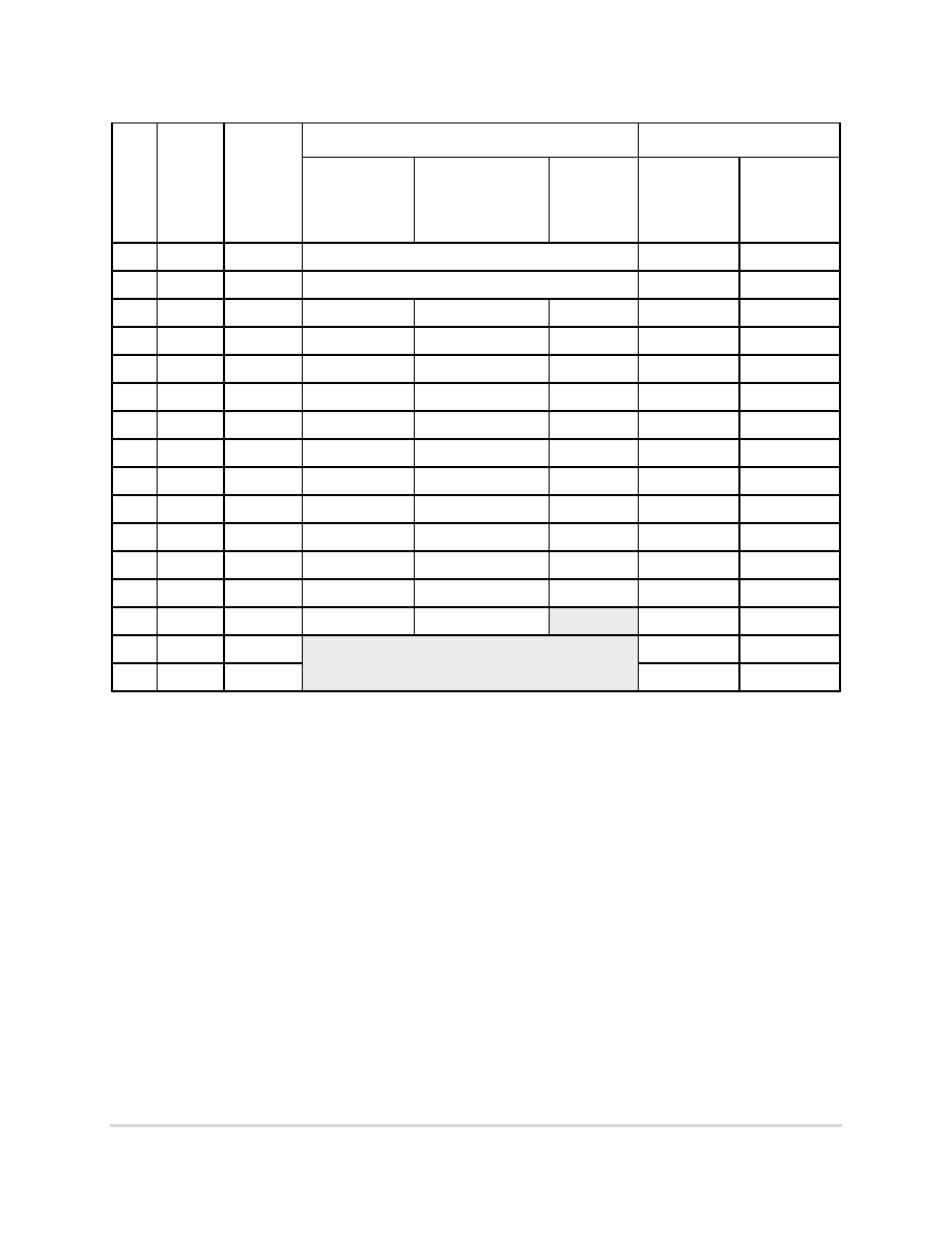
Table 18. MPC8240 Microprocessor PLL Configurations (continued)
Ref.
No.
PLL_
CFG
[0:4] 2
CPU 1
HID1[0:4]
250-MHz Part 8, 9
Ratios 3, 4
PCI Clock Input
(PCI_SYNC_IN)
Range (MHz)
Peripheral
Logic/Mem
Bus Clock Range
(MHz)
CPU Clock
Range
(MHz)
PCI to Mem
(Mem VCO)
Multiplier
Mem to CPU
(CPU VCO)
Multiplier
F
re
e
sc
a
le
S
e
m
ic
o
n
d
u
c
to
r,
I
Freescale Semiconductor, Inc.
For More Information On This Product,
Go to: www.freescale.com
n
c
..
.
相關PDF資料 |
PDF描述 |
|---|---|
| XQ6SLX150T-3CSG484I | IC FPGA SPARTAN-6Q 484-CSBGA |
| XR16C2550IJ-F | IC UART FIFO 16B DUAL 44PLCC |
| XR16C2850IM-F | IC UART FIFO 128B DUAL 48TQFP |
| XR16C2852IJ-F | IC UART FIFO 128B 44PLCC |
| XR16C850IMTR-F | IC UART FIFO 128B 48TQFP |
相關代理商/技術參數 |
參數描述 |
|---|---|
| XPC8241LZP166 | 制造商:未知廠家 制造商全稱:未知廠家 功能描述:Microprocessor |
| XPC8241LZP200 | 制造商:未知廠家 制造商全稱:未知廠家 功能描述:Microprocessor |
| XPC8241TXXX | 制造商:FREESCALE 制造商全稱:Freescale Semiconductor, Inc 功能描述:Intergrated Processor Hardware Specifications |
| XPC8241TZP166B | 制造商:FREESCALE 制造商全稱:Freescale Semiconductor, Inc 功能描述:Intergrated Processor Hardware Specifications |
| XPC8241TZP200B | 制造商:FREESCALE 制造商全稱:Freescale Semiconductor, Inc 功能描述:Intergrated Processor Hardware Specifications |
發(fā)布緊急采購,3分鐘左右您將得到回復。