- 您現(xiàn)在的位置:買賣IC網(wǎng) > PDF目錄203626 > W3E16M72S-200BI (MICROSEMI CORP-PMG MICROELECTRONICS) 16M X 72 DDR DRAM, 0.8 ns, PBGA219 PDF資料下載
參數(shù)資料
| 型號: | W3E16M72S-200BI |
| 廠商: | MICROSEMI CORP-PMG MICROELECTRONICS |
| 元件分類: | DRAM |
| 英文描述: | 16M X 72 DDR DRAM, 0.8 ns, PBGA219 |
| 封裝: | 32 X 25 MM, PLASTIC, BGA-219 |
| 文件頁數(shù): | 15/17頁 |
| 文件大小: | 766K |
| 代理商: | W3E16M72S-200BI |
7
White Electronic Designs Corporation (602) 437-1520 www.whiteedc.com
White Electronic Designs
W3E16M72S-XBX
February 2005
Rev. 7
DESELECT
The DESELECT function (CS# HiGH) prevents new
commands from being executed by the DDR SDRAM.
The SDRAM is effectively deselected. Operations already
in progress are not affected.
NO OPERATION (NOP)
The NO OPERATION (NOP) command is used to perform
a NOP to the selected DDR SDRAM (CS# is LOW). This
prevents unwanted commands from being registered
during idle or wait states. Operations already in progress
are not affected.
LOAD MODE REGISTER
The Mode Registers are loaded via inputs A0-12. The
LOAD MODE REGISTER command can only be issued
when all banks are idle, and a subsequent executable
command cannot be issued until tMRD is met.
ACTIVE
The ACTIVE command is used to open (or activate) a row in
a particular bank for a subsequent access. The value on the
BA0, BA1 inputs selects the bank, and the address provided
COMMAND
READ
NOP
CL = 2.5
DON'T CARE
TRANSITIONING DATA
DQ
DQS
T0
T1
T2
T2n
T3
T3n
COMMAND
READ
NOP
CL = 2
DQ
DQS
CLK
T0
T1
T2
T2n
T3
T3n
Burst Length = 4 in the cases shown
Shown with nominal tAC and nominal tDSDQ
DATA
CLK
OUTPUT DRIVE STRENGTH
The normal full drive strength for all outputs are specied to
be SSTL2, Class II. The DDR SDRAM supports an option
for reduced drive. This option is intended for the support
of the lighter load and/or point-to-point environments. The
selection of the reduced drive strength will alter the DQs
and DQSs from SSTL2, Class II drive strength to a reduced
drive strength, which is approximately 54 percent of the
SSTL2, Class II drive strength.
DLL ENABLE/DISABLE
The DLL must be enabled for normal operation. DLL enable
is required during power-up initialization and upon returning
to normal operation after having disabled the DLL for the
purpose of debug or evaluation. (When the device exits self
refresh mode, the DLL is enabled automatically.) Any time
the DLL is enabled, 200 clock cycles must occur before a
READ command can be issued.
COMMANDS
The Truth Table provides a quick reference of available
commands. This is followed by a written description of
each command.
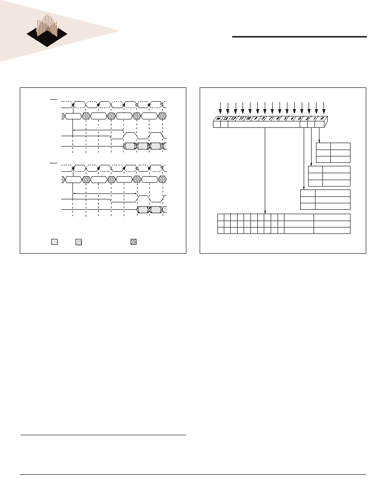
FIGURE 4 – CAS LATENCY
FIGURE 5 – EXTENDED MODE
REGISTER DEFINITION
DLL
Enable
Disable
DLL
DS
A9
A7
A6
A5
A4
A3
A8
A2
A1
A0
Extended Mode
Register (Ex)
Address Bus
Operating Mode
A10
A11
11
01
BA0
BA1
QFC#
E0
0
1
Drive Strength
Normal
Reduced
E1
0
1
QFC# Function
Disabled
Reserved
E22
0
-
Operating Mode
Reserved
E2, E1, E0
Valid
-
E12
0
-
E10
0
-
E9
0
-
E8
0
-
E7
0
-
E6
0
-
E5
0
-
E4
0
-
E3
0
-
A12
E11
0
-
1. E14 and E13 must be "0, 1" to select the Extended Mode Register (vs. the base Mode Register)
2. The QFE# function is not supported.
相關(guān)PDF資料 |
PDF描述 |
|---|---|
| W3E16M72SR-200BM | 16M X 72 DDR DRAM, 0.75 ns, PBGA219 |
| W3E16M72SR-200BC | 16M X 72 DDR DRAM, 0.75 ns, PBGA219 |
| W3E16M72SR-200BM | 16M X 72 DDR DRAM, 0.75 ns, PBGA219 |
| W3EG2128M72AFSR262AD3M | 256M X 72 DDR DRAM MODULE, 0.75 ns, DMA184 |
| W3EG2128M72AFSR335AD3S | 256M X 72 DDR DRAM MODULE, 0.7 ns, DMA184 |
相關(guān)代理商/技術(shù)參數(shù) |
參數(shù)描述 |
|---|---|
| W3E16M72S-200BM | 制造商:WEDC 制造商全稱:White Electronic Designs Corporation 功能描述:16Mx72 DDR SDRAM |
| W3E16M72S-250BC | 制造商:Microsemi Corporation 功能描述:16M X 72 DDR, 2.5V, 250 MHZ, 219 PBGA, COMMERCIAL TEMP. - Bulk |
| W3E16M72S-250BI | 制造商:Microsemi Corporation 功能描述:16M X 72 DDR, 2.5V, 250 MHZ, 219 PBGA, INDUSTRIAL TEMP. - Bulk |
| W3E16M72S-250BM | 制造商:Microsemi Corporation 功能描述:16M X 72 DDR, 2.5V, 250 MHZ, 219 PBGA, MIL-TEMP. - Bulk |
| W3E16M72S-266BC | 制造商:Microsemi Corporation 功能描述:16M X 72 DDR, 2.5V, 266 MHZ, 219 PBGA, COMMERCIAL TEMP. - Bulk |
發(fā)布緊急采購,3分鐘左右您將得到回復(fù)。