- 您現(xiàn)在的位置:買賣IC網(wǎng) > PDF目錄359432 > VSC8164QR (VITESSE SEMICONDUCTOR CORP) AA/9V REMOTE ALMOND BOX PDF資料下載
參數(shù)資料
| 型號(hào): | VSC8164QR |
| 廠商: | VITESSE SEMICONDUCTOR CORP |
| 元件分類: | 數(shù)字傳輸電路 |
| 英文描述: | AA/9V REMOTE ALMOND BOX |
| 中文描述: | MUX/DEMUX, PQFP128 |
| 封裝: | 14 X 20 MM, HEAT SINK, PLASTIC, QFP-128 |
| 文件頁數(shù): | 3/16頁 |
| 文件大小: | 153K |
| 代理商: | VSC8164QR |
VITESSE
reliminary Datasheet
SC8164
2.488 Gbit/sec to 2.7Gbit/sec
1:16 SONET/SDH Demux
G52239-0, Rev. 3.3
5/17/00
VITESSE
SEMICONDUCTOR CORPORATION
741 Calle Plano, Camarillo, CA 93012
805/388-3700
FAX: 805/987-5896
Page 3
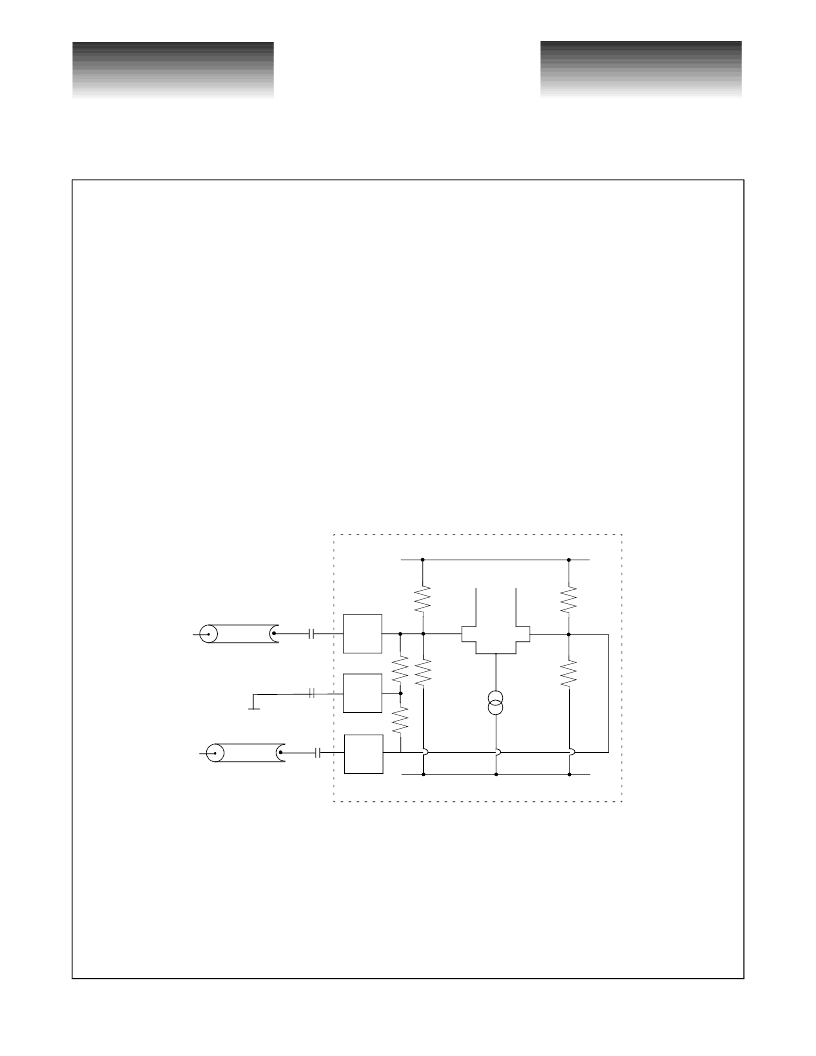
High Speed Interface
The incoming 2.488Gb/s data (up to 2.7Gb/s for FEC applications) and input clock are received by high
speed inputs DI and HSCLKI. The data and clock inputs are internally terminated by a center-tapped resistor
network. For differential input DC coupling, the network is terminated to the appropriate termination voltage
V
Term
(pins HSDREF, HSCLKREF) providing a 50
to
V
Term
termination for both true and complement inputs.
For differential input AC coupling, the network is terminated to
V
Term
via a blocking capacitor.
In most situations these inputs will have high transition density and little DC offset. However, in cases
where this does not hold, direct DC connection is possible. All serial data and clock inputs have the same circuit
topology, as shown in Figure 4. The reference voltage is created by a resistor divider as shown. If the input sig-
nal is driven differentially and DC-coupled to the part, the mid-point of the input signal swing should be cen-
tered about this reference voltage and not exceed the maximum allowable amplitude (
V
CMI
,
V
IHSDC
)
. For
single-ended, DC-coupling operations, it is recommended that the user provides an external reference voltage
which has better temperature and power supply noise rejection than the on-chip resistor divider. The external
reference should have a nominal value equivalent to the common mode switch point of the DC coupled signal,
and can be connected to either side of the differential gate.
Figure 4: High Speed Serial Clock and Data Inputs
Supplies
This device is specified as a LVPECL device with a single positive 3.3V supply. Should the user desire to
use the device in a ECL environment with a negative 3.3V supply, then VCC will be ground and VEE will be -
3.3V.
V
CC
= 3.3V
V
EE
= 0V
C
IN
Chip Boundary
C
IN
TYP = 100 nF
C
AC
TYP = 100 nF
Z
O
V
Term
C
AC
50
50
C
IN
Z
O
相關(guān)PDF資料 |
PDF描述 |
|---|---|
| VSC8166 | 2.488 Gbit/sec 1:16 SONET/SDH Demux with Clock Recovery |
| VSC8169 | OC-48 (FEC) 16:1 SONET/SDH MUX with Clock Generator |
| VSC8171 | SONET/SDH 16:1 Mux with CMU |
| VSC8184 | 11.5-12.5Gb/s 1:16 Demultiplexer with Clock Recovery |
| VSC8211 | Single Port 10/100/1000BASE-T PHY and 1000BASE-X PHY with SGMII, SerDes, GMII, MII, TBI, RGMII / RTBI MAC Interfaces |
相關(guān)代理商/技術(shù)參數(shù) |
參數(shù)描述 |
|---|---|
| VSC8166 | 制造商:VITESSE 制造商全稱:Vitesse Semiconductor Corporation 功能描述:2.488 Gbit/sec 1:16 SONET/SDH Demux with Clock Recovery |
| VSC8169 | 制造商:VITESSE 制造商全稱:Vitesse Semiconductor Corporation 功能描述:OC-48 (FEC) 16:1 SONET/SDH MUX with Clock Generator |
| VSC8169QR | 制造商:VITESSE 制造商全稱:Vitesse Semiconductor Corporation 功能描述:OC-48 (FEC) 16:1 SONET/SDH MUX with Clock Generator |
| VSC8171 | 制造商:VITESSE 制造商全稱:Vitesse Semiconductor Corporation 功能描述:SONET/SDH 16:1 Mux with CMU |
| VSC8172 | 制造商:VITESSE 制造商全稱:Vitesse Semiconductor Corporation 功能描述:SONET/SDH 16:1 Mux with CMU |
發(fā)布緊急采購(gòu),3分鐘左右您將得到回復(fù)。