- 您現(xiàn)在的位置:買賣IC網(wǎng) > PDF目錄1971 > USB-I2C-DIL (Flexipanel)IC USB SYNC SRL I2C 28-DIL PDF資料下載
參數(shù)資料
| 型號: | USB-I2C-DIL |
| 廠商: | Flexipanel |
| 文件頁數(shù): | 8/9頁 |
| 文件大小: | 0K |
| 描述: | IC USB SYNC SRL I2C 28-DIL |
| 標(biāo)準(zhǔn)包裝: | 25 |
| 應(yīng)用: | USB |
| 接口: | I²C |
| 電源電壓: | 1.8 V ~ 5 V |
| 封裝/外殼: | 28-DIP |
| 供應(yīng)商設(shè)備封裝: | 28-DIL |
| 包裝: | 散裝 |
| 安裝類型: | 通孔 |
| 其它名稱: | 658-1036-5 |
p8 of 9
26-Aug-10
USB-SPI
HW144-8
www.hexwax.com
Customization
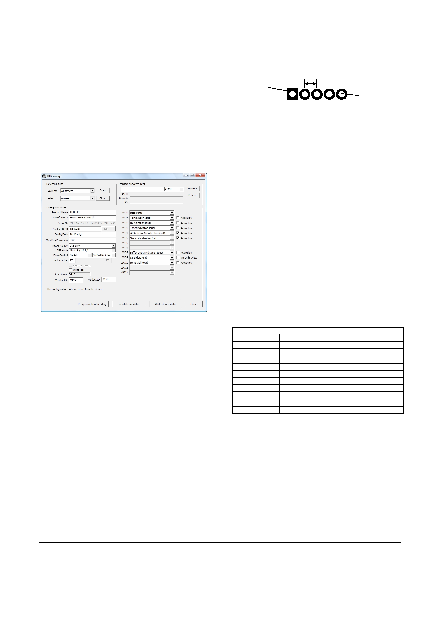
The product can be customized in one of three ways:
1.
Using the HIDconfig.exe application (figure 8) in
the development kit. This application makes it
very easy to copy the configuration from an
existing product to a new product and is suitable
for in-factory use. (It cannot be used if you have
changed the Vendor ID and / Product ID.)
2.
By requesting the custom settings to be supplied
pre-programmed when buying pre-programmed
chips (5K units minimum).
3.
Using customization commands. Documentation
on these commands is available on request.
Figure 8. HIDconfig.exe application
Delivery and Programming
USB-I2C is available pre-programmed in 28-pin DIL and
20-pin SSOP packages. USB-I2C-SS (SSOP package)
may be supplied with an ID label, or it may be identified
with a blue mark on the package.
In high volumes (5K+), USB-I2C is available reeled with
your custom settings preloaded, in any available
package.
TEAclipper Programming
If practical, a TEAclipper programming socket should be
added to the circuit board in order to facilitate in-circuit
firmware updates.
During programming, these connections must be
protected against contention. In particular, note that
Vpp is subject to 13V during programming. Nothing else
should be connected to Vpp except via a 22k pull-up
resistor.
The TEAclipper connector format is shown in figure 9.
Since the programming time is fast, no programming
socket is required.
The TEAclipper can be ‘leaned’
against the plate-through holes shown.
It is strongly recommended that this connector is
included in circuits even if in-circuit programming is not
anticipated, since this allows you to upgrade the
firmware if necessary.
1mm hole dia
2.54mm spacing
Pin 1 indicated
by square pad
P
G
D
P
G
C
V
pp
V
ss
V
dd
Figure 9. Recommended plate-through connector design
Evaluation Board
USB-I2C may be evaluated with the Firmware Factory
USB Products Eval Board (figure 10). The components
which must be fitted are shown in table 5. In addition,
the following connections must be made:
- Jumper A to Jumper C.
- Active low LED to pin 3 (RA1) pf U7.
- Active high pushbutton to pin 4 (RA2) pf U7.
- Pin VIO9 / Send to Vdd.
- Jumper J to Jumper K (20 pin device only)
- Jumper L to Jumper M (20 pin device only)
The prototyping area on the left of the board may be
used to add the LED and pushbutton. In figure 11, an
active low LED has been connected to the AllSysGo#
pin and active high LEDs to the Tx and Rx indicators,
and a jumper provided on the Send input.
(Some
connections are on the underside of the board.)
The printed circuit board integrates an edge connector
of USB Type A format. This may be plugged into a USB
extension cable.
Table 5. Evaluation Board bill of materials
Label
Component
U2
USB-I2C-DIL
U7
PIC18F2321
D2
Wire link
C4d, C6
100nF capacitor
C7
10uF capacitor
C8
470nF capacitor
C2, C3
22pF capacitor
X1
12MHz parallel cut crystal
R2, R3
22k resistor
R4, R5
4k7 resistor
The PIC18F2331 serves as an I2C master for the
evaluation. When the pushbutton is pressed, the LED
lights. Eight bytes are then sent to USB-I2C and eight
bytes are read from USB-I2C. The first time the button
is pressed, the bytes 12 34 56 78 9A BC DE F0 are sent.
Thereafter, the previously received eight bytes are
echoed back. The source code for the I2C host is in the
development kit.
相關(guān)PDF資料 |
PDF描述 |
|---|---|
| USB-SPI-DIL | IC USB SYNC SRL SPI 28-DIL |
| USB2SERA10CFK | USB TO SERIAL BRIDGE |
| V62/11608-01XE | IC SWITCH SPDT SGL 8PIN |
| VNC2-64Q1B-TRAY | IC USB HOST/DEVICE CTRL 64-QFN |
| W78E858A40FL | IC MCU 8-BIT 32K FLASH 44-PQFP |
相關(guān)代理商/技術(shù)參數(shù) |
參數(shù)描述 |
|---|---|
| USB-I2C-SS | 功能描述:USB 接口集成電路 Driver-free USB to serl SPIslve intrfce RoHS:否 制造商:Cypress Semiconductor 產(chǎn)品:USB 2.0 數(shù)據(jù)速率: 接口類型:SPI 工作電源電壓:3.15 V to 3.45 V 工作電源電流: 最大工作溫度:+ 85 C 安裝風(fēng)格:SMD/SMT 封裝 / 箱體:WLCSP-20 |
| USB-ICP-80C51ISP | 功能描述:程序設(shè)計器 - 基于處理器 In-System Programmer for NXP 80C51ISP RoHS:否 制造商:Olimex Ltd. 產(chǎn)品:Programmers 工具用于評估:XMEGA, MegaAVR, tinyAVR 核心:AVR 接口類型:USB 工作電源電壓:1.8 V to 5.5 V |
| USB-ICP-LPC2K | 功能描述:程序設(shè)計器 - 基于處理器 In-System Programmer for NXP ARM7 LPC2xxx RoHS:否 制造商:Olimex Ltd. 產(chǎn)品:Programmers 工具用于評估:XMEGA, MegaAVR, tinyAVR 核心:AVR 接口類型:USB 工作電源電壓:1.8 V to 5.5 V |
| USB-ICP-LPC9XX | 功能描述:程序設(shè)計器 - 基于處理器 In-Circuit Programer for NXP LPC9xx RoHS:否 制造商:Olimex Ltd. 產(chǎn)品:Programmers 工具用于評估:XMEGA, MegaAVR, tinyAVR 核心:AVR 接口類型:USB 工作電源電壓:1.8 V to 5.5 V |
| USB-ICP-SAB9 | 功能描述:插座和適配器 Socket Adapter Brd USB-ICP-LPC9xx Drvr RoHS:否 制造商:Silicon Labs 產(chǎn)品:Adapter 用于:EM35x |
發(fā)布緊急采購,3分鐘左右您將得到回復(fù)。