- 您現(xiàn)在的位置:買賣IC網(wǎng) > PDF目錄383968 > UC5613DPTR Terminator PDF資料下載
參數(shù)資料
| 型號(hào): | UC5613DPTR |
| 英文描述: | Terminator |
| 中文描述: | 終結(jié)者 |
| 文件頁(yè)數(shù): | 3/5頁(yè) |
| 文件大小: | 301K |
| 代理商: | UC5613DPTR |
PARAMETER
TEST CONDITIONS
MIN
TYP
MAX
UNITS
Supply Current Section
Termpwr Supply Current
All termination lines = Open
All termination lines = 0.5V
DISCNCT = Open
17
200
100
23
225
150
mA
mA
μ
A
Power Down Mode
Output Section (Termination Lines)
Terminator Impedance
Output High Voltage
Max Output Current
I
LINE
= -5mA to -15mA
104.5
2.65
-20.3
-19.8
-19.5
-19.0
-21.6
110
2.9
-21.5
-21.5
-21.5
-21.5
-24.0
10
115.5
3.1
-22.4
-22.4
-22.4
-22.4
-25.4
400
100
400
6
Ohms
V
mA
mA
mA
mA
mA
nA
μ
A
nA
pF
V
LINE
= 0.5V
T
J
= 25
°
C
0°C < T
J
< 70°C
T
J
= 25
°
C
0°C < T
J
< 70°C
0°C < T
J
< 70°C
V
LINE
= 0 to 4V
V
LINE
= 5.25V
Max Output Current
V
LINE
= 0.5V, TRMPWR = 4V (Note 1)
V
LINE
= 0.2V, TRMPWR = 4V to 5.25V
DISCNCT = 4V
TRMPWR = 0V to 5.25V
Output Leakage
REG = 0V
REG = Open V
LINE
= 0V to 5.25V
10
5
Output Capacitance
Regulator Section
Regulator Output Voltage
DISCNCT = Open (Note 2) (DP Package)
2.7
2.7
2.9
2.9
10
1.0
-400
100
170
10
3.1
3.1
20
1.2
-600
400
V
V
All Termination Lines = 4V
TRMPWR = 4V to 6V
All Termination Lines = 0.5V
REG = 0V
REG = 3.5V
Line Regulation
Drop Out Voltage
Short Circuit Current
Sinking Current Capability
Thermal Shutdown
Thermal Shutdown Hysteresis
Disconnect Section
Disconnect Threshold
Input Current
mV
V
mA
mA
°C
°C
-200
75
1.1
1.4
-10
1.7
-20
V
μ
A
DISCNCT = 0V
ELECTRICAL CHARACTERISTICS
Unless otherwise stated, these specifications apply for T
A
= 0°C to 70°C.
TRMPWR = 4.75V, DISCNCT = 0V, T
A
= T
J
.
UC5612
Note 1: Measuring each termination line while other 8 are low.
Note 2: Guaranteed by design. Not 100% tested in production.
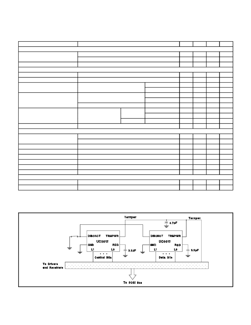
Figure 1: Typical SCSI Bus Configurations Utilizing 2 UC5612 Devices
APPLICATION INFORMATION
UDG-94134
3
Powered by ICminer.com Electronic-Library Service CopyRight 2003
相關(guān)PDF資料 |
PDF描述 |
|---|---|
| UC5613J | Terminator |
| UC5613N | 1.5 A, Very low drop voltage regulators |
| UC5613PWP | 1.5 A, Very low drop voltage regulators |
| UC5613PWPTR | 1.5 A, Very low drop voltage regulators |
| UCC5510MWP | Dual operational amplifier and voltage reference |
相關(guān)代理商/技術(shù)參數(shù) |
參數(shù)描述 |
|---|---|
| UC5613J | 制造商:未知廠家 制造商全稱:未知廠家 功能描述:Terminator |
| UC5613N | 制造商:未知廠家 制造商全稱:未知廠家 功能描述:Terminator |
| UC5613PWP | 制造商:Rochester Electronics LLC 功能描述:- Bulk |
| UC5613PWPTR | 制造商:未知廠家 制造商全稱:未知廠家 功能描述:Terminator |
| UC563DP | 功能描述:視頻 IC 32line VME Bus RoHS:否 制造商:Fairchild Semiconductor 工作電源電壓:5 V 電源電流:80 mA 最大工作溫度:+ 85 C 封裝 / 箱體:TSSOP-28 封裝:Reel |
發(fā)布緊急采購(gòu),3分鐘左右您將得到回復(fù)。