- 您現(xiàn)在的位置:買賣IC網(wǎng) > PDF目錄359758 > TSC251G2DXXX-24CB IC CYCLONE III FPGA 80K 484 FBGA PDF資料下載
參數(shù)資料
| 型號(hào): | TSC251G2DXXX-24CB |
| 英文描述: | IC CYCLONE III FPGA 80K 484 FBGA |
| 中文描述: | 微控制器 |
| 文件頁(yè)數(shù): | 7/63頁(yè) |
| 文件大小: | 878K |
| 代理商: | TSC251G2DXXX-24CB |
第1頁(yè)第2頁(yè)第3頁(yè)第4頁(yè)第5頁(yè)第6頁(yè)當(dāng)前第7頁(yè)第8頁(yè)第9頁(yè)第10頁(yè)第11頁(yè)第12頁(yè)第13頁(yè)第14頁(yè)第15頁(yè)第16頁(yè)第17頁(yè)第18頁(yè)第19頁(yè)第20頁(yè)第21頁(yè)第22頁(yè)第23頁(yè)第24頁(yè)第25頁(yè)第26頁(yè)第27頁(yè)第28頁(yè)第29頁(yè)第30頁(yè)第31頁(yè)第32頁(yè)第33頁(yè)第34頁(yè)第35頁(yè)第36頁(yè)第37頁(yè)第38頁(yè)第39頁(yè)第40頁(yè)第41頁(yè)第42頁(yè)第43頁(yè)第44頁(yè)第45頁(yè)第46頁(yè)第47頁(yè)第48頁(yè)第49頁(yè)第50頁(yè)第51頁(yè)第52頁(yè)第53頁(yè)第54頁(yè)第55頁(yè)第56頁(yè)第57頁(yè)第58頁(yè)第59頁(yè)第60頁(yè)第61頁(yè)第62頁(yè)第63頁(yè)
Rev. A - May 7, 1999
7
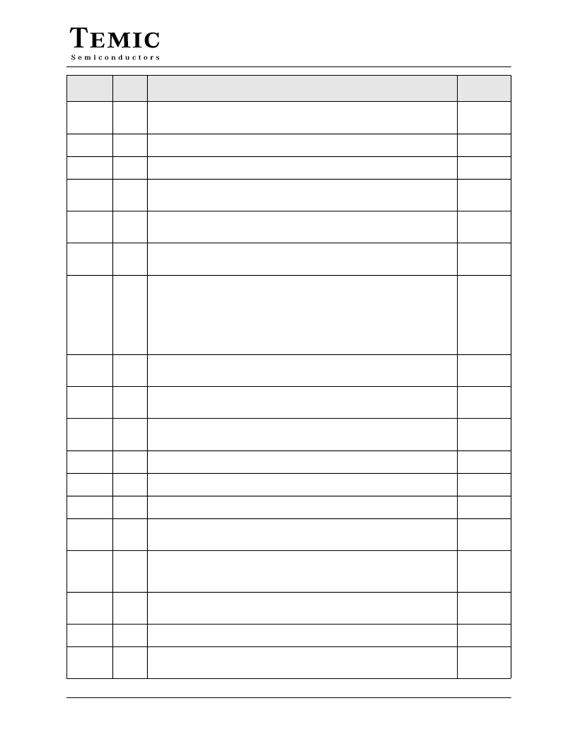
TSC80251G2D
P1.0:7
I/O
Port 1
P1 is an 8-bit bidirectional I/O port with internal pull-ups. P1 provides interrupt capability
for a keyboard interface.
P2.0:7
I/O
Port 2
P2 is an 8-bit bidirectional I/O port with internal pull-ups.
A15:8
P3.0:7
I/O
Port 3
P3 is an 8-bit bidirectional I/O port with internal pull-ups.
PROG#
I
Programming Pulse input
The programming pulse is applied to this input for programming the on-chip EPROM/
OTPROM.
PSEN#
O
Program Store Enable/Read signal output
PSEN# is asserted for a memory address range that depends on bits RD0 and RD1 in
UCONFIG0 byte (see Table 13, Page 15).
Read or 17
th
Address Bit (A16)
Read signal output to external data memory depending on the values of bits RD0 and RD1
in UCONFIG0 byte (see Table 13, Page 15).
RD#
O
P3.7
RST
I
Reset input to the chip
Holding this pin high for 64 oscillator periods while the oscillator is running resets the device.
The Port pins are driven to their reset conditions when a voltage greater than V
IH1
is applied,
whether or not the oscillator is running.
This pin has an internal pull-down resistor which allows the device to be reset by connecting
a capacitor between this pin and VDD.
Asserting RST when the chip is in Idle mode or Power-Down mode returns the chip to normal
operation.
RXD
I/O
Receive Serial Data
RXD sends and receives data in serial I/O mode 0 and receives data in serial I/O modes 1,
2 and 3.
I
2
C Serial Clock
When I
2
C controller is in master mode, SCL outputs the serial clock to slave peripherals.
When I
2
C controller is in slave mode, SCL receives clock from the master controller.
P3.0
SCL
I/O
P1.6
SCK
I/O
SPI Serial Clock
When SPI is in master mode, SCK outputs clock to the slave peripheral. When SPI is in
slave mode, SCK receives clock from the master controller.
I
2
C Serial Data
SDA is the bidirectional I
2
C data line.
P1.6
SDA
I/O
P1.7
SS#
I
SPI Slave Select Input
When in Slave mode, SS# enables the slave mode.
P1.4
T1:0
I/O
Timer 1:0 External Clock Inputs
When timer 1:0 operates as a counter, a falling edge on the T1:0 pin increments the count.
T2
I/O
Timer 2 Clock Input/Output
For the timer 2 capture mode, T2 is the external clock input. For the Timer 2 clock-out mode,
T2 is the clock output.
P1.0
T2EX
I
Timer 2 External Input
In timer 2 capture mode, a falling edge initiates a capture of the timer 2 registers. In auto-
reload mode, a falling edge causes the timer 2 register to be reloaded. In the up-down counter
mode, this signal determines the count direction: 1= up, 0= down.
P1.1
TXD
O
Transmit Serial Data
TXD outputs the shift clock in serial I/O mode 0 and transmits data in serial I/O modes 1,
2 and 3.
P3.1
VDD
PWR
Digital Supply Voltage
Connect this pin to +5V or +3V supply voltage.
VPP
I
Programming Supply Voltage
The programming supply voltage is applied to this input for programming the on-chip EPROM/
OTPROM.
Signal
Name
Type
Description
Alternate
Function
相關(guān)PDF資料 |
PDF描述 |
|---|---|
| TSC251G2DXXX-24CED | IC CYCLONE III FPGA 80K 484 FBGA |
| TSC251G2DXXX-24IA | IC CYCLONE III FPGA 80K 484 FBGA |
| TSC251G2DXXX-24IB | IC CYCLONE III FPGA 80K 780FBGA |
| TSC251G2DXXX-L16CB | IC CYCLONE III FPGA 80K 780FBGA |
| TSC251G2DXXX-L16CED | IC CYCLONE III FPGA 80K 780FBGA |
相關(guān)代理商/技術(shù)參數(shù) |
參數(shù)描述 |
|---|---|
| TSC251G2DXXX-24CE | 制造商:ATMEL 制造商全稱:ATMEL Corporation 功能描述:8/16-bit Microcontroller with Serial Communication Interfaces |
| TSC251G2DXXX-24CED | 制造商:未知廠家 制造商全稱:未知廠家 功能描述:Microcontroller |
| TSC251G2DXXX-24IA | 制造商:ATMEL 制造商全稱:ATMEL Corporation 功能描述:8/16-bit Microcontroller with Serial Communication Interfaces |
| TSC251G2DXXX-24IB | 制造商:ATMEL 制造商全稱:ATMEL Corporation 功能描述:8/16-bit Microcontroller with Serial Communication Interfaces |
| TSC251G2DXXX-L16CB | 制造商:ATMEL 制造商全稱:ATMEL Corporation 功能描述:8/16-bit Microcontroller with Serial Communication Interfaces |
發(fā)布緊急采購(gòu),3分鐘左右您將得到回復(fù)。