- 您現(xiàn)在的位置:買賣IC網(wǎng) > PDF目錄382635 > TMS320F2810PGFAEP (Texas Instruments, Inc.) Digital Signal Processors PDF資料下載
參數(shù)資料
| 型號: | TMS320F2810PGFAEP |
| 廠商: | Texas Instruments, Inc. |
| 元件分類: | 數(shù)字信號處理 |
| 英文描述: | Digital Signal Processors |
| 中文描述: | 數(shù)字信號處理器 |
| 文件頁數(shù): | 63/159頁 |
| 文件大小: | 2084K |
| 代理商: | TMS320F2810PGFAEP |
第1頁第2頁第3頁第4頁第5頁第6頁第7頁第8頁第9頁第10頁第11頁第12頁第13頁第14頁第15頁第16頁第17頁第18頁第19頁第20頁第21頁第22頁第23頁第24頁第25頁第26頁第27頁第28頁第29頁第30頁第31頁第32頁第33頁第34頁第35頁第36頁第37頁第38頁第39頁第40頁第41頁第42頁第43頁第44頁第45頁第46頁第47頁第48頁第49頁第50頁第51頁第52頁第53頁第54頁第55頁第56頁第57頁第58頁第59頁第60頁第61頁第62頁當前第63頁第64頁第65頁第66頁第67頁第68頁第69頁第70頁第71頁第72頁第73頁第74頁第75頁第76頁第77頁第78頁第79頁第80頁第81頁第82頁第83頁第84頁第85頁第86頁第87頁第88頁第89頁第90頁第91頁第92頁第93頁第94頁第95頁第96頁第97頁第98頁第99頁第100頁第101頁第102頁第103頁第104頁第105頁第106頁第107頁第108頁第109頁第110頁第111頁第112頁第113頁第114頁第115頁第116頁第117頁第118頁第119頁第120頁第121頁第122頁第123頁第124頁第125頁第126頁第127頁第128頁第129頁第130頁第131頁第132頁第133頁第134頁第135頁第136頁第137頁第138頁第139頁第140頁第141頁第142頁第143頁第144頁第145頁第146頁第147頁第148頁第149頁第150頁第151頁第152頁第153頁第154頁第155頁第156頁第157頁第158頁第159頁
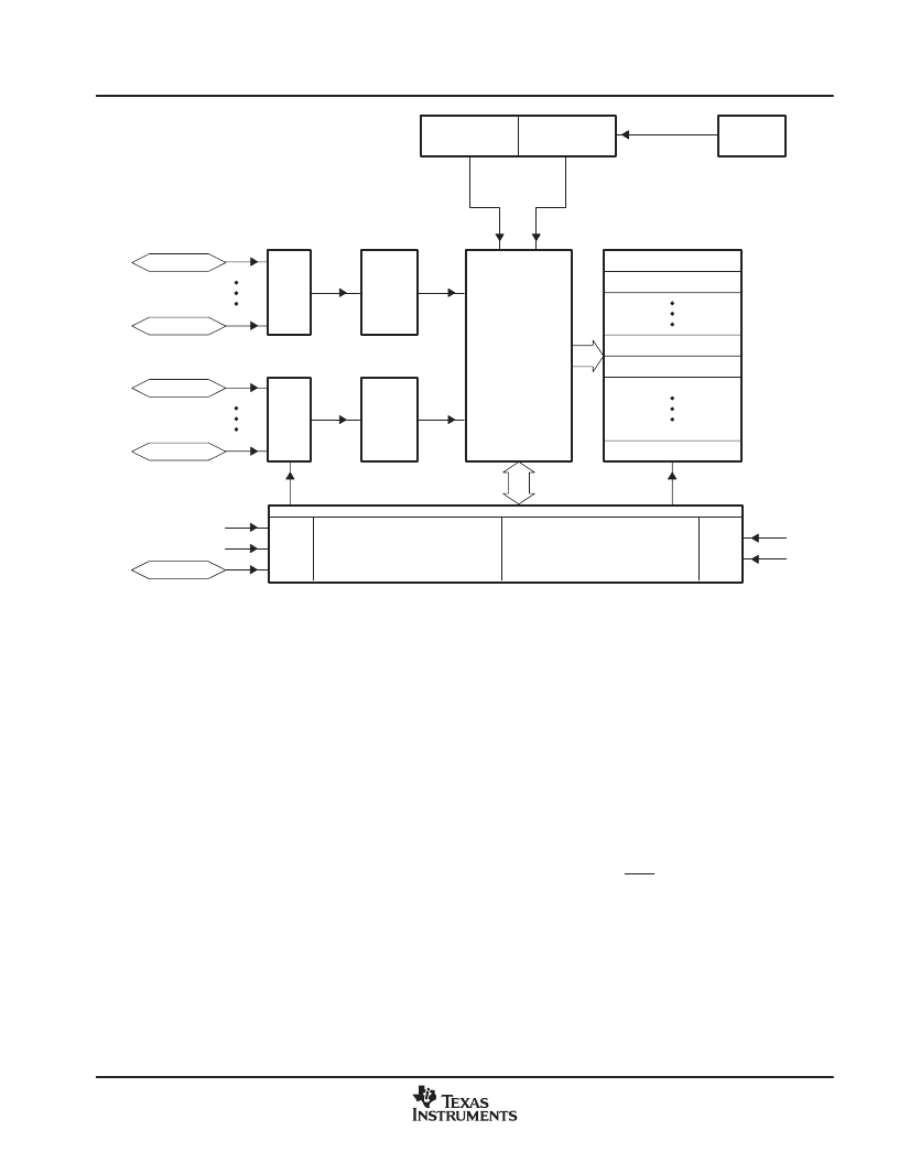
Peripherals
63
March 2004 Revised October 2004
SGUS051A
Result Registers
EVB
S/W
ADCSOC
EVA
S/W
Sequencer 2
Sequencer 1
SOC
SOC
ADC Control Registers
70B7h
70B0h
70AFh
70A8h
Result Reg 15
Result Reg 8
Result Reg 7
Result Reg 1
Result Reg 0
Module
ADC
12-Bit
Analog
MUX
ADCINA0
ADCINA7
ADCINB0
ADCINB7
System
Control Block
High-Speed
Prescaler
HSPCLK
ADCENCLK
C28x
SYSCLKOUT
S/H
S/H
Figure 44. Block Diagram of the F281x and C281x ADC Module
To obtain the specified accuracy of the ADC, proper board layout is very critical. To the best extent possible,
traces leading to the ADCIN pins should not run in close proximity to the digital signal paths. This is to minimize
switching noise on the digital lines from getting coupled to the ADC inputs. Furthermore, proper isolation
techniques must be used to isolate the ADC module power pins (V
DDA1
/V
DDA2
, AV
DDREFBG
) from the digital
supply. Figure 45 shows the ADC pin connections for the F281x and C281x devices.
Notes:
1.
The ADC registers are accessed at the SYSCLKOUT rate. The internal timing of the ADC module is
controlled by the high-speed peripheral clock (HSPCLK).
2.
The behavior of the ADC module based on the state of the ADCENCLK and HALT signals is as follows:
ADCENCLK:
On reset, this signal will be low. While reset is active-low (XRS) the clock to the register will
still function. This is necessary to make sure all registers and modes go into their default reset state. The
analog module will however be in a low-power inactive state. As soon as reset goes high, then the clock to
the registers will be disabled. When the user sets the ADCENCLK signal high, then the clocks to the
registers will be enabled and the analog module will be enabled. There will be a certain time delay (ms
range) before the ADC is stable and can be used.
HALT:
This signal only affects the analog module. It does not affect the registers. If low, the ADC module is
powered. If high, the ADC module goes into low-power mode. The HALT mode will stop the clock to the
CPU, which will stop the HSPCLK. Therefore the ADC register logic will be turned off indirectly.
相關PDF資料 |
PDF描述 |
|---|---|
| TMX20F2810PBKAEP | Digital Signal Processors |
| TMS320LC2404APGA | DSP CONTROLLERS |
| TMP320LC2401APAGA | DSP CONTROLLERS |
| TMP320LC2401APAGS | DSP CONTROLLERS |
| TMP320LC2401APGA | DSP CONTROLLERS |
相關代理商/技術參數(shù) |
參數(shù)描述 |
|---|---|
| TMS320F2811PBKA | 功能描述:數(shù)字信號處理器和控制器 - DSP, DSC 32-Bit Digital Sig Controller w/Flash RoHS:否 制造商:Microchip Technology 核心:dsPIC 數(shù)據(jù)總線寬度:16 bit 程序存儲器大小:16 KB 數(shù)據(jù) RAM 大小:2 KB 最大時鐘頻率:40 MHz 可編程輸入/輸出端數(shù)量:35 定時器數(shù)量:3 設備每秒兆指令數(shù):50 MIPs 工作電源電壓:3.3 V 最大工作溫度:+ 85 C 封裝 / 箱體:TQFP-44 安裝風格:SMD/SMT |
| TMS320F2811PBKA | 制造商:Texas Instruments 功能描述:DIGITAL SIGNAL PROCESSOR |
| TMS320F2811PBKACG-19A4NYW | 制造商:Texas Instruments 功能描述: |
| TMS320F2811PBKQ | 功能描述:數(shù)字信號處理器和控制器 - DSP, DSC 32-Bit Digital Sig Controller w/Flash RoHS:否 制造商:Microchip Technology 核心:dsPIC 數(shù)據(jù)總線寬度:16 bit 程序存儲器大小:16 KB 數(shù)據(jù) RAM 大小:2 KB 最大時鐘頻率:40 MHz 可編程輸入/輸出端數(shù)量:35 定時器數(shù)量:3 設備每秒兆指令數(shù):50 MIPs 工作電源電壓:3.3 V 最大工作溫度:+ 85 C 封裝 / 箱體:TQFP-44 安裝風格:SMD/SMT |
| TMS320F2811PBKS | 功能描述:數(shù)字信號處理器和控制器 - DSP, DSC 32-Bit Digital Sig Controller w/Flash RoHS:否 制造商:Microchip Technology 核心:dsPIC 數(shù)據(jù)總線寬度:16 bit 程序存儲器大小:16 KB 數(shù)據(jù) RAM 大小:2 KB 最大時鐘頻率:40 MHz 可編程輸入/輸出端數(shù)量:35 定時器數(shù)量:3 設備每秒兆指令數(shù):50 MIPs 工作電源電壓:3.3 V 最大工作溫度:+ 85 C 封裝 / 箱體:TQFP-44 安裝風格:SMD/SMT |
發(fā)布緊急采購,3分鐘左右您將得到回復。