- 您現(xiàn)在的位置:買賣IC網 > PDF目錄383961 > TMS320C6421_0711 (Texas Instruments, Inc.) Fixed-Point Digital Signal Processor PDF資料下載
參數(shù)資料
| 型號: | TMS320C6421_0711 |
| 廠商: | Texas Instruments, Inc. |
| 元件分類: | 數(shù)字信號處理 |
| 英文描述: | Fixed-Point Digital Signal Processor |
| 中文描述: | 定點數(shù)字信號處理器 |
| 文件頁數(shù): | 103/223頁 |
| 文件大小: | 1658K |
| 代理商: | TMS320C6421_0711 |
第1頁第2頁第3頁第4頁第5頁第6頁第7頁第8頁第9頁第10頁第11頁第12頁第13頁第14頁第15頁第16頁第17頁第18頁第19頁第20頁第21頁第22頁第23頁第24頁第25頁第26頁第27頁第28頁第29頁第30頁第31頁第32頁第33頁第34頁第35頁第36頁第37頁第38頁第39頁第40頁第41頁第42頁第43頁第44頁第45頁第46頁第47頁第48頁第49頁第50頁第51頁第52頁第53頁第54頁第55頁第56頁第57頁第58頁第59頁第60頁第61頁第62頁第63頁第64頁第65頁第66頁第67頁第68頁第69頁第70頁第71頁第72頁第73頁第74頁第75頁第76頁第77頁第78頁第79頁第80頁第81頁第82頁第83頁第84頁第85頁第86頁第87頁第88頁第89頁第90頁第91頁第92頁第93頁第94頁第95頁第96頁第97頁第98頁第99頁第100頁第101頁第102頁當前第103頁第104頁第105頁第106頁第107頁第108頁第109頁第110頁第111頁第112頁第113頁第114頁第115頁第116頁第117頁第118頁第119頁第120頁第121頁第122頁第123頁第124頁第125頁第126頁第127頁第128頁第129頁第130頁第131頁第132頁第133頁第134頁第135頁第136頁第137頁第138頁第139頁第140頁第141頁第142頁第143頁第144頁第145頁第146頁第147頁第148頁第149頁第150頁第151頁第152頁第153頁第154頁第155頁第156頁第157頁第158頁第159頁第160頁第161頁第162頁第163頁第164頁第165頁第166頁第167頁第168頁第169頁第170頁第171頁第172頁第173頁第174頁第175頁第176頁第177頁第178頁第179頁第180頁第181頁第182頁第183頁第184頁第185頁第186頁第187頁第188頁第189頁第190頁第191頁第192頁第193頁第194頁第195頁第196頁第197頁第198頁第199頁第200頁第201頁第202頁第203頁第204頁第205頁第206頁第207頁第208頁第209頁第210頁第211頁第212頁第213頁第214頁第215頁第216頁第217頁第218頁第219頁第220頁第221頁第222頁第223頁
www.ti.com
TMS320C6421
Fixed-Point Digital Signal Processor
SPRS346C–JANUARY 2007–REVISED NOVEMBER 2007
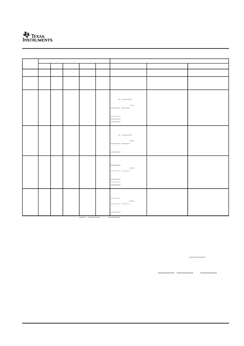
Table 3-37. EMIFA Block Major Configuration Choices
MAJ OR
CONFIG.
OPTION
PINMUX SELECTION FIELDS
RESULTING PERIPHERALS/PINS
AEM
RMII
CS3SEL
CS4SEL
CS5SEL
EMIFA
(1)
RMII
GPIO
58 GP Pins:
GP[96:89], GP[54:5]
A
000
0
0
0
0
-
-
RMII:
RMRXER, RMRXD[1:0],
RMTXD[1:0], REFCLK,
RMCRSDV, RMTXEN
50 GP Pins:
GP[96:89], GP[54:53],
GP[51:34], GP[26:5],
B
000
1
0
0
0
-
8-bit EMIFA (Async) Pinout
Mode 2:
EM_A[21:0], EM_D[7:0],
EM_R/W, EM_CS2,
EM_BA[1:0],
EM_WAIT/(RDY/BSY),
EM_WE, EM_OE
13 GP pins:
GP[54:52], GP[31:22]
Optional Selection:
GP[33] (CS5SEL = 0),
GP[32] (CS4SEL = 0),
GP[13] (CS3SEL = 0)
C
010
0
0 or 1
0 or 1
0 or 1
-
Optional Selection:
EM_CS5 (CS5SEL = 1),
EM_CS4 (CS4SEL = 1),
EM_CS3 (CS3SEL = 1)
8-bit EMIFA (Async) Pinout
Mode 2:
EM_A[21:0], EM_D[7:0],
EM_R/W, EM_CS2,
EM_BA[1:0],
EM_WAIT/(RDY/BSY),
EM_WE, EM_OE
7 GP pins:
GP[54:53], GP[26:22]
RMII:
RMRXER, RMRXD[1:0],
RMTXD[1:0], REFCLK,
RMCRSDV, RMTXEN
D
010
1
0 or 1
0
0
Optional Selection:
GP[13] (CS3SEL = 0)
Optional Selection:
EM_CS3 (CS3SEL = 1)
8-bit EMIFA (NAND) Pinout
Mode 5:
EM_D[7:0], EM_A[2:1],
EM_CS2,
EM_WAIT/(RDY/BSY),
EM_WE, EM_OE
44 GP pins:
GP[96:89], GP[54:34],
GP[31:22], GP[11:10],
GP[7:5]
E
101
0
0 or 1
0 or 1
0 or 1
-
Optional Selection:
GP[33] (CS5SEL = 0),
GP[32] (CS4SEL = 0),
GP[13] (CS3SEL = 0)
Optional Selection:
EM_CS5 (CS5SEL = 1),
EM_CS4 (CS4SEL = 1),
EM_CS3 (CS3SEL = 1)
8-bit EMIFA (NAND) Pinout
Mode 5:
EM_D[7:0], EM_A[2:1],
EM_CS2,
EM_WAIT/(RDY/BSY),
EM_WE, EM_OE
38 GP pins:
GP[96:89], GP[54:34],
GP[26:22], GP[11:10],
GP[7:5]
RMII:
RMRXER, RMRXD[1:0],
RMTXD[1:0], REFCLK,
RMCRSDV, RMTXEN
F
101
1
0 or 1
0
0
Optional Selection:
GP[13] (CS3SEL = 0)
Optional Selection:
EM_CS3 (CS3SEL = 1)
(1)
The EMIFA pins EM_WAIT/(RDY/BSY), EM_OE, and EM_WE are non-multiplexed pins. They are available in all the configuration
options. However, they are only useful if additional EMIFA pins are functional. Therefore in this table, these pins are only listed in
configuration options C,D,E, and F.
The following is an example on how to read
Table 3-37
. For example, the "PINMUX Selection Fields"
columns indicate that Major Configuration Choice C is selected through setting PINMUX0.AEM = 010b
and PINMUX0.RMII = 0. Other PINMUX0 fields CS3SEL, CS4SEL, and CS5SEL can be set to either 0 or
1 based on the system's EMIFA Chip Select space need. The "Resulting Peripherals/Pins" columns
indicate that Major Configuration Option C can support the following combination of pin functions:
Pins for 8-bit EMIFA (Async or NAND) function with EMIFA Chip Select space 2 (EM_CS2). If
additional Chip Select spaces are needed, set the corresponding PINMUX bit (CS5SEL, CS4SEL,
and/or CS3SEL) to 1.
At least 13 GPIO pins. If the additional Chip Select spaces from EM_CS3, EM_CS4, or EM_CS5 are
not needed, the corresponding PINMUX bit (CS3SEL, CS4SEL, and/or CS5SEL) can be set to 0 to get
additional GPIO pins.
3.7.3.11.2
EMIFA Block Pin-By-Pin Multiplexing Summary
This section summarizes the EMIFA Block muxing on a pin-by-pin basis. It provides an alternative view to
pin muxing in the EMIFA Block. It summarizes the EMIFA Block pin muxing by dividing up the EMIFA
Block based on the PINMUX field that controls the pins. To determine the actual EMIFA Major
Configuration Option for the application need, see
Section 3.7.3.11.1
,
EMIFA Block Major Configuration
Choices
.
Submit Documentation Feedback
Device Configurations
103
相關PDF資料 |
PDF描述 |
|---|---|
| TMS320C6421_07 | Fixed-Point Digital Signal Processor |
| TMS320DM6437ZDU5 | Digital Media Processor |
| TMX320DM6437AZDUA | Digital Media Processor |
| TMX320DM6437BZDUA | Digital Media Processor |
| TMX320DM6437BZWTA | Digital Media Processor |
相關代理商/技術參數(shù) |
參數(shù)描述 |
|---|---|
| TMS320C64217WTL | 制造商:Texas Instruments 功能描述: |
| TMS320C6421ZDU4 | 功能描述:數(shù)字信號處理器和控制器 - DSP, DSC Fixed-Pt Dig Signal Proc RoHS:否 制造商:Microchip Technology 核心:dsPIC 數(shù)據總線寬度:16 bit 程序存儲器大小:16 KB 數(shù)據 RAM 大小:2 KB 最大時鐘頻率:40 MHz 可編程輸入/輸出端數(shù)量:35 定時器數(shù)量:3 設備每秒兆指令數(shù):50 MIPs 工作電源電壓:3.3 V 最大工作溫度:+ 85 C 封裝 / 箱體:TQFP-44 安裝風格:SMD/SMT |
| TMS320C6421ZDU5 | 功能描述:數(shù)字信號處理器和控制器 - DSP, DSC TMS6421 ZDU PKG 500 RoHS:否 制造商:Microchip Technology 核心:dsPIC 數(shù)據總線寬度:16 bit 程序存儲器大小:16 KB 數(shù)據 RAM 大小:2 KB 最大時鐘頻率:40 MHz 可編程輸入/輸出端數(shù)量:35 定時器數(shù)量:3 設備每秒兆指令數(shù):50 MIPs 工作電源電壓:3.3 V 最大工作溫度:+ 85 C 封裝 / 箱體:TQFP-44 安裝風格:SMD/SMT |
| TMS320C6421ZDU6 | 功能描述:數(shù)字信號處理器和控制器 - DSP, DSC Fixed-Point Dig Signal Processor RoHS:否 制造商:Microchip Technology 核心:dsPIC 數(shù)據總線寬度:16 bit 程序存儲器大小:16 KB 數(shù)據 RAM 大小:2 KB 最大時鐘頻率:40 MHz 可編程輸入/輸出端數(shù)量:35 定時器數(shù)量:3 設備每秒兆指令數(shù):50 MIPs 工作電源電壓:3.3 V 最大工作溫度:+ 85 C 封裝 / 箱體:TQFP-44 安裝風格:SMD/SMT |
| TMS320C6421ZDU7 | 功能描述:數(shù)字信號處理器和控制器 - DSP, DSC Fixed-Pt Dig Signal Proc RoHS:否 制造商:Microchip Technology 核心:dsPIC 數(shù)據總線寬度:16 bit 程序存儲器大小:16 KB 數(shù)據 RAM 大小:2 KB 最大時鐘頻率:40 MHz 可編程輸入/輸出端數(shù)量:35 定時器數(shù)量:3 設備每秒兆指令數(shù):50 MIPs 工作電源電壓:3.3 V 最大工作溫度:+ 85 C 封裝 / 箱體:TQFP-44 安裝風格:SMD/SMT |
發(fā)布緊急采購,3分鐘左右您將得到回復。