- 您現(xiàn)在的位置:買賣IC網(wǎng) > PDF目錄384019 > TMP320F28044ZGMS (Texas Instruments, Inc.) Digital Signal Processor PDF資料下載
參數(shù)資料
| 型號: | TMP320F28044ZGMS |
| 廠商: | Texas Instruments, Inc. |
| 元件分類: | 數(shù)字信號處理 |
| 英文描述: | Digital Signal Processor |
| 中文描述: | 數(shù)字信號處理器 |
| 文件頁數(shù): | 89/107頁 |
| 文件大小: | 784K |
| 代理商: | TMP320F28044ZGMS |
第1頁第2頁第3頁第4頁第5頁第6頁第7頁第8頁第9頁第10頁第11頁第12頁第13頁第14頁第15頁第16頁第17頁第18頁第19頁第20頁第21頁第22頁第23頁第24頁第25頁第26頁第27頁第28頁第29頁第30頁第31頁第32頁第33頁第34頁第35頁第36頁第37頁第38頁第39頁第40頁第41頁第42頁第43頁第44頁第45頁第46頁第47頁第48頁第49頁第50頁第51頁第52頁第53頁第54頁第55頁第56頁第57頁第58頁第59頁第60頁第61頁第62頁第63頁第64頁第65頁第66頁第67頁第68頁第69頁第70頁第71頁第72頁第73頁第74頁第75頁第76頁第77頁第78頁第79頁第80頁第81頁第82頁第83頁第84頁第85頁第86頁第87頁第88頁當(dāng)前第89頁第90頁第91頁第92頁第93頁第94頁第95頁第96頁第97頁第98頁第99頁第100頁第101頁第102頁第103頁第104頁第105頁第106頁第107頁
www.ti.com
ADCSOCAO
or
ADCSOCBO
t
w(ADCSOCAL)
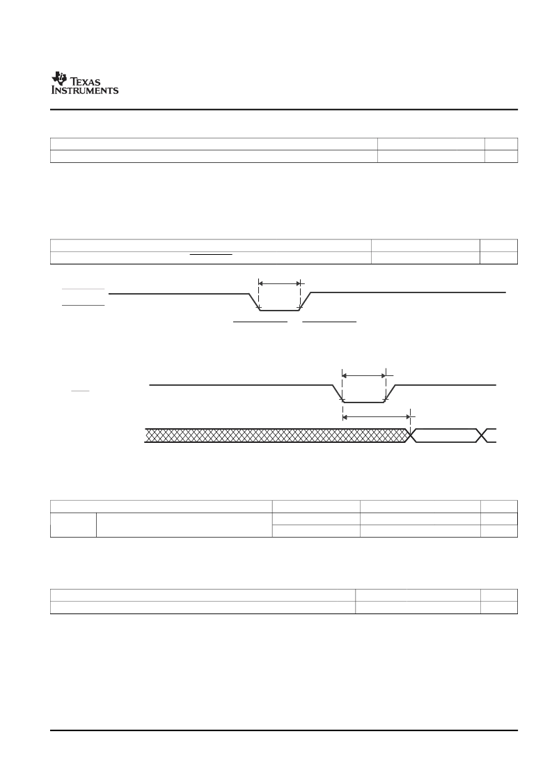
6.10.3 External Interrupt Timing
XNMI, XINT1, XINT2
t
w(INT)
Interrupt Vector
t
d(INT)
Address bus
(internal)
TMS320F28044
Digital Signal Processor
SPRS357B–AUGUST 2006–REVISED MAY 2007
Table 6-21. High Resolution PWM Characteristics at SYSCLKOUT = (60 - 100 MHz)
MIN
TYP
150
MAX
310
UNIT
ps
Micro Edge Positioning (MEP) step size
(1)
(1)
Maximum MEP step size is based on worst-case process, maximum temperature and maximum voltage. MEP step size will increase
with low voltage and high temperature and decrease with voltage and cold temperature.
Applications that use the HRPWM feature should use MEP Scale Factor Optimizer (SFO) estimation software functions. See the TI
software libraries for details of using SFO function in end applications. SFO functions help to estimate the number of MEP steps per
SYSCLKOUT period dynamically while the HRPWM is in operation.
Table 6-22. External ADC Start-of-Conversion Switching Characteristics
PARAMETER
Pulse duration, ADCSOCAO low
MIN
MAX
UNIT
cycles
t
w(ADCSOCAL)
32t
c(HCO)
Figure 6-14. ADCSOCAO or ADCSOCBO Timing
Figure 6-15. External Interrupt Timing
Table 6-23. External Interrupt Timing Requirements
(1)
TEST CONDITIONS
Synchronous
With qualifier
MIN
MAX
UNIT
cycles
cycles
t
w(INT)(2)
Pulse duration, INT input low/high
1t
c(SCO)
1t
c(SCO)
+ t
w(IQSW)
(1)
(2)
For an explanation of the input qualifier parameters, see
Table 6-11
.
This timing is applicable to any GPIO pin configured for ADCSOC functionality.
Table 6-24. External Interrupt Switching Characteristics
(1)
PARAMETER
MIN
MAX
UNIT
cycles
t
d(INT)
(1)
Delay time, INT low/high to interrupt-vector fetch
t
w(IQSW)
+ 12t
c(SCO)
For an explanation of the input qualifier parameters, see
Table 6-11
.
Submit Documentation Feedback
Electrical Specifications
89
相關(guān)PDF資料 |
PDF描述 |
|---|---|
| TMS320F28044_07 | Digital Signal Processor |
| TMS320F28044ZGMA | Digital Signal Processor |
| TMS320F28044ZGMQ | Digital Signal Processor |
| TMS320F28044ZGMS | Digital Signal Processor |
| TMX320F28044GGMQ | Digital Signal Processor |
相關(guān)代理商/技術(shù)參數(shù) |
參數(shù)描述 |
|---|---|
| TMP320F2810GHHA | 制造商:TI 制造商全稱:Texas Instruments 功能描述:DIGITAL SIGNAL PROCESSORS |
| TMP320F2810GHHMEP | 制造商:TI 制造商全稱:Texas Instruments 功能描述:Digital Signal Processors |
| TMP320F2810GHHS | 制造商:TI 制造商全稱:Texas Instruments 功能描述:DIGITAL SIGNAL PROCESSORS |
| TMP320F2810PBKA | 制造商:Texas Instruments 功能描述: |
| TMP320F2810PBKAEP | 制造商:TI 制造商全稱:Texas Instruments 功能描述:Digital Signal Processors |
發(fā)布緊急采購,3分鐘左右您將得到回復(fù)。