- 您現(xiàn)在的位置:買賣IC網(wǎng) > PDF目錄383959 > TMC3533R2C80 (FAIRCHILD SEMICONDUCTOR CORP) Triple Video D/A Converter 8 bit, 80 Msps, 3.3V PDF資料下載
參數(shù)資料
| 型號(hào): | TMC3533R2C80 |
| 廠商: | FAIRCHILD SEMICONDUCTOR CORP |
| 元件分類: | DAC |
| 英文描述: | Triple Video D/A Converter 8 bit, 80 Msps, 3.3V |
| 中文描述: | TRIPLE, PARALLEL, 8 BITS INPUT LOADING, 0.015 us SETTLING TIME, 8-BIT DAC, PQCC44 |
| 封裝: | PLASTIC, LCC-44 |
| 文件頁(yè)數(shù): | 9/12頁(yè) |
| 文件大小: | 68K |
| 代理商: | TMC3533R2C80 |
PRODUCT SPECIFICATION
TMC3533
REV. 0.9.1 11/24/99
9
Application Notes
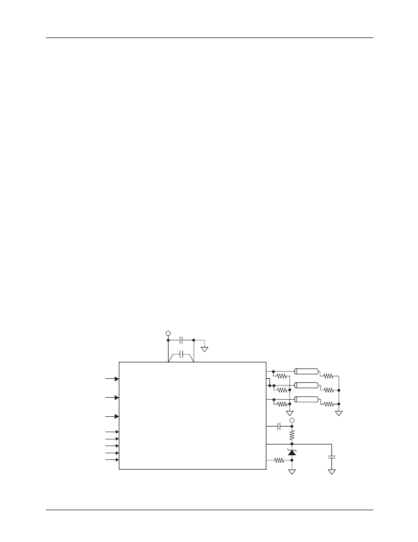
Figure 4 illustrates a typical TMC3533 interface circuit. In
this example, an optional 1.2 Volt bandgap reference is con-
nected to the V
REF
output, overriding the internal voltage
reference source.
Grounding
It is important that the TMC3533 power supply is well-regu-
lated and free of high-frequency noise. Careful power supply
decoupling will ensure the highest quality video signals at
the output of the circuit. The TMC3533 has separate analog
and digital circuits. To keep digital system noise from the
D/A converter, it is recommended that power supply voltages
(V
DD
) come from the system analog power source and all
ground connections (GND) be made to the analog ground
plane. Power supply pins should be individually decoupled
at the pin.
Printed Circuit Board Layout
Designing with high-performance mixed-signal circuits
demands printed circuits with ground planes. Overall system
performance is strongly influenced by the board layout.
Capacitive coupling from digital to analog circuits may
result in poor D/A conversion. Consider the following sug-
gestions when doing the layout:
1.
Keep the critical analog traces (V
REF
, I
REF
, COMP,
IO
S
, IO
R
, IO
G
, IO
B
) as short as possible and as far as
possible from all digital signals. The TMC3533 should
be located near the board edge, close to the analog out-
put connectors.
2.
The power plane for the TMC3533 should be separate
from that which supplies the digital circuitry. A single
power plane
should be used for all of the V
DD
pins. If
the power supply for the TMC3533 is the same as that of
the system's digital circuitry, power to the TMC3533
should be decoupled with 0.1μF and 0.01μF capacitors
and isolated with a ferrite bead.
3.
The ground plane should be solid, not cross-hatched.
Connections to the ground plane should have very short
leads.
4.
If the digital power supply has a dedicated power plane
layer, it should not be placed under the TMC3533, the
voltage reference, or the analog outputs. Capacitive cou-
pling of digital power supply noise from this layer to the
TMC3533 and its related analog circuitry can have an
adverse effect on performance.
5.
CLK should be handled carefully. Jitter and noise on
this clock will degrade performance. Terminate the
clock line carefully to eliminate overshoot and ringing.
Related Products
TMC3003 Triple 10-bit 80 Msps D/A Converter
TMC2242C/TMC2243/TMC2246A Video Filters
TMC2081 Digital Video Mixer
TMC3503 Triple Video D/A Converter, 5V
TMC22x5y Video Decoder
Figure 4. Typical Interface Circuit
65-3533-05
R7-0
G7-0
B7-0
+3.3V
0.1
μ
F
10
μ
F
VDD
GND
TMC3533
Triple 8-bit
D/A Converter
CLK
SYNC
BLANK
WHITE
SLEEP
RED PIXEL
INPUT
GREEN PIXEL
INPUT
BLUE PIXEL
INPUT
CLOCK
SYNC
BLANK
WHITE
SLEEP
COMP
VREF
RREF
+3.3V
0.1
μ
F
0.1
μ
F
572
3.3k
LM185-1.2
(Optional)
IOR
IOS
IOG
IOB
75
75
75
75
75
75
ZO=75
ZO=75
Blue
ZO=75
Red
Green w/Sync
相關(guān)PDF資料 |
PDF描述 |
|---|---|
| TMC3533KRC30 | Triple Video D/A Converter 8 bit, 80 Msps, 3.3V |
| TMC3533KRC50 | Triple Video D/A Converter 8 bit, 80 Msps, 3.3V |
| TMC3533KRC80 | Triple Video D/A Converter 8 bit, 80 Msps, 3.3V |
| TMC3533 | ECONOLINE: RSZ/P - 1kVDC |
| TMC3533R2C30 | Triple Video D/A Converter 8 bit, 80 Msps, 3.3V |
相關(guān)代理商/技術(shù)參數(shù) |
參數(shù)描述 |
|---|---|
| TMC37X37BR2 | 功能描述:電線導(dǎo)管 SLOTTD DUCTLOWSMOKE 37MMX37MMX2MBR RoHS:否 制造商:Panduit 類型:Slotted SideWall Open finger design wiring cut 材料:Polypropylene 顏色:Light Gray 大小: 最大光束直徑: 抗拉強(qiáng)度: 外部導(dǎo)管寬度:25 mm 外部導(dǎo)管高度:25 mm |
| TMC389-EVAL | 制造商:Trinamic 功能描述:Bulk |
| TMC389-LA | 制造商:Trinamic 功能描述:IC BRIDGE DRIVER SPI/PAR 32QFN 制造商:Trinamic 功能描述:STEPPER DRIVER 3-PHASE 6A QFN32 |
| TMC4 | 制造商:Hubbell Premise Wiring 功能描述: |
| TMC40 | 制造商:TRUMPOWER 制造商全稱:Tumbler Technologies + TRUMPower 功能描述:30-48 WATT MEDICAL & ITE SWITCHING POWER SUPPLIES |
發(fā)布緊急采購(gòu),3分鐘左右您將得到回復(fù)。