- 您現(xiàn)在的位置:買賣IC網(wǎng) > PDF目錄383959 > TMC3533R2C80 (FAIRCHILD SEMICONDUCTOR CORP) Triple Video D/A Converter 8 bit, 80 Msps, 3.3V PDF資料下載
參數(shù)資料
| 型號(hào): | TMC3533R2C80 |
| 廠商: | FAIRCHILD SEMICONDUCTOR CORP |
| 元件分類: | DAC |
| 英文描述: | Triple Video D/A Converter 8 bit, 80 Msps, 3.3V |
| 中文描述: | TRIPLE, PARALLEL, 8 BITS INPUT LOADING, 0.015 us SETTLING TIME, 8-BIT DAC, PQCC44 |
| 封裝: | PLASTIC, LCC-44 |
| 文件頁(yè)數(shù): | 4/12頁(yè) |
| 文件大小: | 68K |
| 代理商: | TMC3533R2C80 |
TMC3533
PRODUCT SPECIFICATION
4
REV. 0.9.1 11/24/99
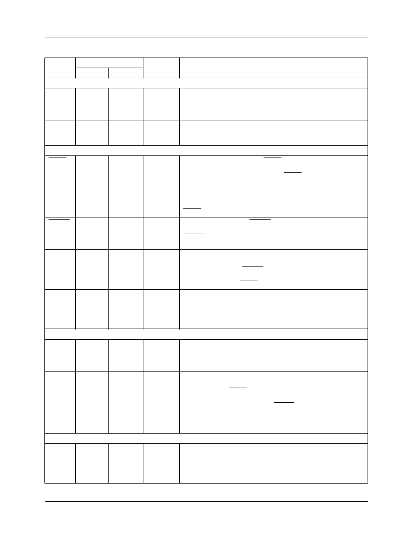
Pin Descriptions
Pin
Name
Clock and Pixel I/O
CLK
Pin Number
LQFP
Value
Pin Function Description
PLCC
26
27
TTL
Clock Input.
The clock input is TTL-compatible and all pixel
data is registered on the rising edge of CLK. It is recommended
that CLK be driven by a dedicated TTL buffer to avoid reflection
induced jitter, overshoot, and undershoot.
Red, Green, and Blue Pixel Inputs.
The R, G, and B digital
inputs are TTL-compatible and registered on the rising edge of
CLK.
R
7-0
G
7-0
B
7-0
Controls
SYNC
47-40
9-2
23-16
6-1, 44-43
14-7
25-18
TTL
11
16
TTL
Sync Pulse Input.
Bringing SYNC LOW, turns off a 40 IRE
(7.62 mA) current source which forms a sync pulse on any D/A
converter output connected to IO
S
. SYNC is registered on the
rising edge of CLK along with pixel data and has the same
pipeline latency as BLANK and pixel data. SYNC does not
override any other data and should be used only during the
blanking interval. If the system does not require sync pulses,
SYNC and IO
S
should be connected to GND.
Blanking Input.
When BLANK is LOW, pixel inputs are ignored
and the D/A converter outputs are driven to the blanking level.
BLANK is registered on the rising edge of CLK and has the
same two-pipe latency as SYNC and Data.
Force Full Scale Input.
When WHITE is HIGH, pixel inputs are
ignored and the D/A converter outputs are driven to their full-
scale output level. A BLANK input overwrites a WHITE input.
WHITE is register on the rising edge of CLK and has the same
two-pipe latency as SYNC and Data.
Power-down Control Input.
When HIGH, SLEEP places the D/
A converter in a low-power-dissipation mode. The D/A current
sources and the digital processing are disabled. The last data
loaded into the input and D/A registers is retained. This control is
asynchronous.
BLANK
10
15
TTL
WHITE
—
26
TTL
SLEEP
—
28
TTL
Video Outputs
IO
R
IO
G
IO
B
33
32
29
39
38
33
0.714 V
p-p
Red, Green, and Blue Data Outputs.
The current source
outputs of the D/A converters are capable of driving RS-343A/
SMPTE-170M compatible levels into doubly-terminated 75 Ohm
lines. Sync pulses may be added to any D/A output.
SYNC Current Output.
When this pin is connected to any of the
D/A converter outputs, a 40 IRE offset can be added to the video
level. When the SYNC input is LOW, the current is turned off,
bring the sync tip voltage to 0.0V. If no sync pulse is required,
IO
S
should be grounded. When SYNC is HIGH, the current
flowing out of IO
S
is:
IO
S
32
(connected
to IO
G
)
37
0.714 V
p-p
IO
S
= 3.64 (V
REF
/ R
REF
)
Voltage Reference
V
REF
35
41
+1.235 V
Voltage Reference Input/Output.
An internal voltage source of
+1.235 Volts is output on this pin. An external +1.235 Volt
reference may be applied here which overrides the internal
reference. Decoupling V
REF
to GND with a 0.1μF ceramic
capacitor is required.
相關(guān)PDF資料 |
PDF描述 |
|---|---|
| TMC3533KRC30 | Triple Video D/A Converter 8 bit, 80 Msps, 3.3V |
| TMC3533KRC50 | Triple Video D/A Converter 8 bit, 80 Msps, 3.3V |
| TMC3533KRC80 | Triple Video D/A Converter 8 bit, 80 Msps, 3.3V |
| TMC3533 | ECONOLINE: RSZ/P - 1kVDC |
| TMC3533R2C30 | Triple Video D/A Converter 8 bit, 80 Msps, 3.3V |
相關(guān)代理商/技術(shù)參數(shù) |
參數(shù)描述 |
|---|---|
| TMC37X37BR2 | 功能描述:電線導(dǎo)管 SLOTTD DUCTLOWSMOKE 37MMX37MMX2MBR RoHS:否 制造商:Panduit 類型:Slotted SideWall Open finger design wiring cut 材料:Polypropylene 顏色:Light Gray 大小: 最大光束直徑: 抗拉強(qiáng)度: 外部導(dǎo)管寬度:25 mm 外部導(dǎo)管高度:25 mm |
| TMC389-EVAL | 制造商:Trinamic 功能描述:Bulk |
| TMC389-LA | 制造商:Trinamic 功能描述:IC BRIDGE DRIVER SPI/PAR 32QFN 制造商:Trinamic 功能描述:STEPPER DRIVER 3-PHASE 6A QFN32 |
| TMC4 | 制造商:Hubbell Premise Wiring 功能描述: |
| TMC40 | 制造商:TRUMPOWER 制造商全稱:Tumbler Technologies + TRUMPower 功能描述:30-48 WATT MEDICAL & ITE SWITCHING POWER SUPPLIES |
發(fā)布緊急采購(gòu),3分鐘左右您將得到回復(fù)。