- 您現(xiàn)在的位置:買賣IC網(wǎng) > PDF目錄384003 > TLC2543MEP (Texas Instruments, Inc.) 12-BIT ANALOG-TO-DIGITAL CONVERTER WITH SERIAL CONTROL AND 11 ANALOG INPUTS PDF資料下載
參數(shù)資料
| 型號: | TLC2543MEP |
| 廠商: | Texas Instruments, Inc. |
| 英文描述: | 12-BIT ANALOG-TO-DIGITAL CONVERTER WITH SERIAL CONTROL AND 11 ANALOG INPUTS |
| 中文描述: | 12位模擬數(shù)字轉(zhuǎn)換串行控制和11個模擬輸入 |
| 文件頁數(shù): | 3/25頁 |
| 文件大?。?/td> | 364K |
| 代理商: | TLC2543MEP |
www.ti.com
TLC2543-EP
12-BIT ANALOG-TO-DIGITAL CONVERTER
WITH SERIAL CONTROL AND 11 ANALOG INPUTS
SGLS125A–JULY 2002–REVISED NOVEMBER 2006
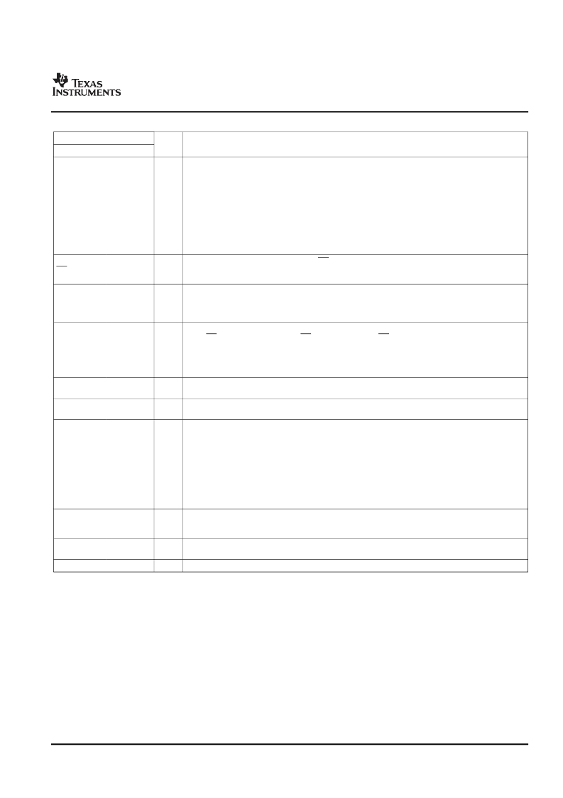
TERMINAL FUNCTIONS
TERMINAL
NAME
AIN0
AIN1
AIN2
AIN3
AIN4
AIN5
AIN6
AIN7
AIN8
AIN9
AIN10
I/O
DESCRIPTION
NO.
1
2
3
4
5
6
7
8
9
11
12
Analog input. These 11 analog-signal inputs are internally multiplexed. The driving source
impedance should be less than or equal to 50
for 4.1-MHz I/O CLOCK operation, and be capable
of slewing the analog input voltage into a capacitance of 60 pF.
I
Chip select. A high-to-low transition on CS resets the internal counters and controls and enables
DATA OUT, DATA INPUT, and I/O CLOCK. A low-to-high transition disables DATA INPUT and I/O
CLOCK within a setup time.
Serial-data input. A 4-bit serial address selects the desired analog input or test voltage to be
converted next. The serial data is presented with the most significant bit (MSB) first and is shifted in
on the first four rising edges of I/O CLOCK. After the four address bits are read into the address
register, I/O CLOCK clocks the remaining bits in order.
The 3-state serial output for the A/D conversion result. DATA OUT is in the high-impedance state
when CS is high and active when CS is low. With a valid CS, DATA OUT is removed from the
high-impedance state and is driven to the logic level corresponding to the most significant bit/least
significant bit (MSB/LSB) value of the previous conversion result. The next falling edge of I/O
CLOCK drives DATA OUT to the logic level corresponding to the next MSB/LSB, and the remaining
bits are shifted out in order.
End of conversion. EOC goes from a high to a low logic level after the falling edge of the last I/O
CLOCK and remains low until the conversion is complete and the data is ready for transfer.
Ground. GND is the ground return terminal for the internal circuitry. Unless otherwise noted, all
voltage measurements are with respect to GND.
Input/output clock. I/O CLOCK receives the serial input and performs the following four functions:
It clocks the eight input data bits into the input data register on the first eight rising edges of I/O
CLOCK with the multiplexer address available after the fourth rising edge.
On the fourth falling edge of I/O CLOCK, the analog input voltage on the selected multiplexer input
begins charging the capacitor array and continues to do so until the last falling edge of the I/O
CLOCK.
It shifts the 11 remaining bits of the previous conversion data out on DATA OUT. Data changes on
the falling edge of I/O CLOCK.
It transfers control of the conversion to the internal state controller on the falling edge of the last
I/O CLOCK.
Positive reference voltage. The upper reference voltage value (nominally V
) is applied to REF+.
The maximum input voltage range is determined by the difference between the voltage applied to
this terminal and the voltage applied to the REF– terminal.
Negative reference voltage. The lower reference voltage value (nominally ground) is applied to
REF–.
Positive supply voltage
CS
15
I
DATA INPUT
17
I
DATA OUT
16
O
EOC
19
O
GND
10
I/O CLOCK
18
I
REF+
14
I
REF–
13
I
V
CC
20
3
Submit Documentation Feedback
相關(guān)PDF資料 |
PDF描述 |
|---|---|
| TLC2543QEP | 12-BIT ANALOG-TO-DIGITAL CONVERTER WITH SERIAL CONTROL AND 11 ANALOG INPUTS |
| TLC2654AIN | Advanced LinCMOSE LOW-NOISE CHOPPER-STABILIZED OPERATIONAL AMPLIFIERS |
| TLC2654AI-14D | Circular Connector; No. of Contacts:26; Series:MS27473; Body Material:Aluminum; Connecting Termination:Crimp; Connector Shell Size:16; Circular Contact Gender:Pin; Circular Shell Style:Straight Plug; Insert Arrangement:16-26 RoHS Compliant: No |
| TLC2654MFK | Advanced LinCMOSE LOW-NOISE CHOPPER-STABILIZED OPERATIONAL AMPLIFIERS |
| TLC2654I-14D | Advanced LinCMOSE LOW-NOISE CHOPPER-STABILIZED OPERATIONAL AMPLIFIERS |
相關(guān)代理商/技術(shù)參數(shù) |
參數(shù)描述 |
|---|---|
| TLC2543MJB | 功能描述:模數(shù)轉(zhuǎn)換器 - ADC 12-Bit A/D w/Serial RoHS:否 制造商:Texas Instruments 通道數(shù)量:2 結(jié)構(gòu):Sigma-Delta 轉(zhuǎn)換速率:125 SPs to 8 KSPs 分辨率:24 bit 輸入類型:Differential 信噪比:107 dB 接口類型:SPI 工作電源電壓:1.7 V to 3.6 V, 2.7 V to 5.25 V 最大工作溫度:+ 85 C 安裝風格:SMD/SMT 封裝 / 箱體:VQFN-32 |
| TLC2543QDWREP | 功能描述:模數(shù)轉(zhuǎn)換器 - ADC 12B Alog/Dig Cnvertr Military Enhanced RoHS:否 制造商:Texas Instruments 通道數(shù)量:2 結(jié)構(gòu):Sigma-Delta 轉(zhuǎn)換速率:125 SPs to 8 KSPs 分辨率:24 bit 輸入類型:Differential 信噪比:107 dB 接口類型:SPI 工作電源電壓:1.7 V to 3.6 V, 2.7 V to 5.25 V 最大工作溫度:+ 85 C 安裝風格:SMD/SMT 封裝 / 箱體:VQFN-32 |
| TLC254ACD | 功能描述:運算放大器 - 運放 Quad LinCMOS RoHS:否 制造商:STMicroelectronics 通道數(shù)量:4 共模抑制比(最小值):63 dB 輸入補償電壓:1 mV 輸入偏流(最大值):10 pA 工作電源電壓:2.7 V to 5.5 V 安裝風格:SMD/SMT 封裝 / 箱體:QFN-16 轉(zhuǎn)換速度:0.89 V/us 關(guān)閉:No 輸出電流:55 mA 最大工作溫度:+ 125 C 封裝:Reel |
| TLC254ACDG4 | 功能描述:運算放大器 - 運放 LinCMOS Quad OP AMP RoHS:否 制造商:STMicroelectronics 通道數(shù)量:4 共模抑制比(最小值):63 dB 輸入補償電壓:1 mV 輸入偏流(最大值):10 pA 工作電源電壓:2.7 V to 5.5 V 安裝風格:SMD/SMT 封裝 / 箱體:QFN-16 轉(zhuǎn)換速度:0.89 V/us 關(guān)閉:No 輸出電流:55 mA 最大工作溫度:+ 125 C 封裝:Reel |
| TLC254ACN | 功能描述:運算放大器 - 運放 Lin CMOS Quad RoHS:否 制造商:STMicroelectronics 通道數(shù)量:4 共模抑制比(最小值):63 dB 輸入補償電壓:1 mV 輸入偏流(最大值):10 pA 工作電源電壓:2.7 V to 5.5 V 安裝風格:SMD/SMT 封裝 / 箱體:QFN-16 轉(zhuǎn)換速度:0.89 V/us 關(guān)閉:No 輸出電流:55 mA 最大工作溫度:+ 125 C 封裝:Reel |
發(fā)布緊急采購,3分鐘左右您將得到回復。