- 您現(xiàn)在的位置:買賣IC網(wǎng) > PDF目錄384003 > TLC2543MEP (Texas Instruments, Inc.) 12-BIT ANALOG-TO-DIGITAL CONVERTER WITH SERIAL CONTROL AND 11 ANALOG INPUTS PDF資料下載
參數(shù)資料
| 型號(hào): | TLC2543MEP |
| 廠商: | Texas Instruments, Inc. |
| 英文描述: | 12-BIT ANALOG-TO-DIGITAL CONVERTER WITH SERIAL CONTROL AND 11 ANALOG INPUTS |
| 中文描述: | 12位模擬數(shù)字轉(zhuǎn)換串行控制和11個(gè)模擬輸入 |
| 文件頁(yè)數(shù): | 17/25頁(yè) |
| 文件大小: | 364K |
| 代理商: | TLC2543MEP |
第1頁(yè)第2頁(yè)第3頁(yè)第4頁(yè)第5頁(yè)第6頁(yè)第7頁(yè)第8頁(yè)第9頁(yè)第10頁(yè)第11頁(yè)第12頁(yè)第13頁(yè)第14頁(yè)第15頁(yè)第16頁(yè)當(dāng)前第17頁(yè)第18頁(yè)第19頁(yè)第20頁(yè)第21頁(yè)第22頁(yè)第23頁(yè)第24頁(yè)第25頁(yè)
www.ti.com
Chip-Select (CS) Input
CS enables and disables the device. During normal operation, CS should be low. Although the use of CS is not
necessary to synchronize a data transfer, it can be brought high between conversions to coordinate the data
transfer of several devices sharing the same bus.
Power-Down Features
When a binary address of 1110 is clocked into the input data register during the first four I/O CLOCK cycles, the
power-down mode is selected. Power down is activated on the falling edge of the fourth I/O CLOCK pulse.
Analog Input, Test, and Power-Down Mode
The 11 analog inputs, 3 internal voltages, and power-down mode are selected by the input multiplexer according
to the input addresses shown in
Table 3
,
Table 4
, and
Table 5
. The input multiplexer is a break-before-make
type to reduce input-to-input noise rejection resulting from channel switching. Sampling of the analog input starts
on the falling edge of the fourth I/O CLOCK and continues for the remaining I/O CLOCK pulses. The sample is
held on the falling edge of the last I/O clock pulse. The three internal test inputs are applied to the multiplexer,
then sampled and converted in the same manner as the external analog inputs. The first conversion after the
device has returned from the power-down state may not read accurately due to internal device settling.
TLC2543-EP
12-BIT ANALOG-TO-DIGITAL CONVERTER
WITH SERIAL CONTROL AND 11 ANALOG INPUTS
SGLS125A–JULY 2002–REVISED NOVEMBER 2006
When CS is brought high, the serial-data output is immediately brought to the high-impedance state, releasing
its output data line to other devices that may share it. After an internally generated debounce time, I/O CLOCK is
inhibited, thus preventing any further change in the internal state.
When CS is subsequently brought low again, the device is reset. CS must be held low for an internal debounce
time before the reset operation takes effect. After CS is debounced low, I/O CLOCK must remain inactive (low)
for a minimum time before a new I/O cycle can start.
CS can interrupt any ongoing data transfer or any ongoing conversion. When CS is debounced low long enough
before the end of the current conversion cycle, the previous conversion result is saved in the internal output
buffer and shifted out during the next I/O cycle.
During power down, all internal circuitry is put in a low-current standby mode. No conversions are performed,
and the internal output buffer keeps the previous conversion cycle data results provided that all digital inputs are
held above V
CC
– 0.5 V or below 0.5 V. The I/O logic remains active so the current I/O cycle must be completed,
even when the power-down mode is selected. Upon power-on reset and before the first I/O cycle, the converter
normally begins in the power-down mode. The device remains in the power-down mode until a valid input
address (other than 1110) is clocked in. Upon completion of that I/O cycle, a normal conversion is performed
with the results being shifted out during the next I/O cycle.
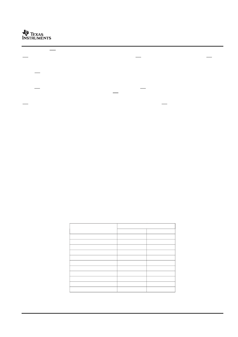
Table 3. Analog-Channel-Select Address
VALUE SHIFTED INTO DATA INPUT
BINARY
0000
0001
0010
0011
0100
0101
0110
0111
1000
1001
1010
ANALOG INPUT
SELECTED
HEX
0
1
2
3
4
5
6
7
8
9
A
AIN0
AIN1
AIN2
AIN3
AIN4
AIN5
AIN6
AIN7
AIN8
AIN9
AIN10
17
Submit Documentation Feedback
相關(guān)PDF資料 |
PDF描述 |
|---|---|
| TLC2543QEP | 12-BIT ANALOG-TO-DIGITAL CONVERTER WITH SERIAL CONTROL AND 11 ANALOG INPUTS |
| TLC2654AIN | Advanced LinCMOSE LOW-NOISE CHOPPER-STABILIZED OPERATIONAL AMPLIFIERS |
| TLC2654AI-14D | Circular Connector; No. of Contacts:26; Series:MS27473; Body Material:Aluminum; Connecting Termination:Crimp; Connector Shell Size:16; Circular Contact Gender:Pin; Circular Shell Style:Straight Plug; Insert Arrangement:16-26 RoHS Compliant: No |
| TLC2654MFK | Advanced LinCMOSE LOW-NOISE CHOPPER-STABILIZED OPERATIONAL AMPLIFIERS |
| TLC2654I-14D | Advanced LinCMOSE LOW-NOISE CHOPPER-STABILIZED OPERATIONAL AMPLIFIERS |
相關(guān)代理商/技術(shù)參數(shù) |
參數(shù)描述 |
|---|---|
| TLC2543MJB | 功能描述:模數(shù)轉(zhuǎn)換器 - ADC 12-Bit A/D w/Serial RoHS:否 制造商:Texas Instruments 通道數(shù)量:2 結(jié)構(gòu):Sigma-Delta 轉(zhuǎn)換速率:125 SPs to 8 KSPs 分辨率:24 bit 輸入類型:Differential 信噪比:107 dB 接口類型:SPI 工作電源電壓:1.7 V to 3.6 V, 2.7 V to 5.25 V 最大工作溫度:+ 85 C 安裝風(fēng)格:SMD/SMT 封裝 / 箱體:VQFN-32 |
| TLC2543QDWREP | 功能描述:模數(shù)轉(zhuǎn)換器 - ADC 12B Alog/Dig Cnvertr Military Enhanced RoHS:否 制造商:Texas Instruments 通道數(shù)量:2 結(jié)構(gòu):Sigma-Delta 轉(zhuǎn)換速率:125 SPs to 8 KSPs 分辨率:24 bit 輸入類型:Differential 信噪比:107 dB 接口類型:SPI 工作電源電壓:1.7 V to 3.6 V, 2.7 V to 5.25 V 最大工作溫度:+ 85 C 安裝風(fēng)格:SMD/SMT 封裝 / 箱體:VQFN-32 |
| TLC254ACD | 功能描述:運(yùn)算放大器 - 運(yùn)放 Quad LinCMOS RoHS:否 制造商:STMicroelectronics 通道數(shù)量:4 共模抑制比(最小值):63 dB 輸入補(bǔ)償電壓:1 mV 輸入偏流(最大值):10 pA 工作電源電壓:2.7 V to 5.5 V 安裝風(fēng)格:SMD/SMT 封裝 / 箱體:QFN-16 轉(zhuǎn)換速度:0.89 V/us 關(guān)閉:No 輸出電流:55 mA 最大工作溫度:+ 125 C 封裝:Reel |
| TLC254ACDG4 | 功能描述:運(yùn)算放大器 - 運(yùn)放 LinCMOS Quad OP AMP RoHS:否 制造商:STMicroelectronics 通道數(shù)量:4 共模抑制比(最小值):63 dB 輸入補(bǔ)償電壓:1 mV 輸入偏流(最大值):10 pA 工作電源電壓:2.7 V to 5.5 V 安裝風(fēng)格:SMD/SMT 封裝 / 箱體:QFN-16 轉(zhuǎn)換速度:0.89 V/us 關(guān)閉:No 輸出電流:55 mA 最大工作溫度:+ 125 C 封裝:Reel |
| TLC254ACN | 功能描述:運(yùn)算放大器 - 運(yùn)放 Lin CMOS Quad RoHS:否 制造商:STMicroelectronics 通道數(shù)量:4 共模抑制比(最小值):63 dB 輸入補(bǔ)償電壓:1 mV 輸入偏流(最大值):10 pA 工作電源電壓:2.7 V to 5.5 V 安裝風(fēng)格:SMD/SMT 封裝 / 箱體:QFN-16 轉(zhuǎn)換速度:0.89 V/us 關(guān)閉:No 輸出電流:55 mA 最大工作溫度:+ 125 C 封裝:Reel |
發(fā)布緊急采購(gòu),3分鐘左右您將得到回復(fù)。