- 您現(xiàn)在的位置:買賣IC網(wǎng) > PDF目錄383952 > TLC251BCD (Texas Instruments, Inc.) LinCMOSE PROGRAMMABLE LOW-POWER OPERATIONAL AMPLIFIERS PDF資料下載
參數(shù)資料
| 型號: | TLC251BCD |
| 廠商: | Texas Instruments, Inc. |
| 英文描述: | LinCMOSE PROGRAMMABLE LOW-POWER OPERATIONAL AMPLIFIERS |
| 中文描述: | LinCMOSE可編程低功耗運算放大器 |
| 文件頁數(shù): | 17/18頁 |
| 文件大小: | 273K |
| 代理商: | TLC251BCD |
TLC251, TLC251A, TLC251B, TLC251Y
LinCMOS
PROGRAMMABLE
LOW-POWER OPERATIONAL AMPLIFIERS
SLOS001E – JULY 1983 – REVISED AUGUST 1994
17
POST OFFICE BOX 655303
DALLAS, TEXAS 75265
APPLICATION INFORMATION
using BIAS SELECT
The TLC251 has a terminal called BIAS SELECT that allows the selection of one of three I
DD
conditions (10,
150, and 1000
μ
A typical). This allows the user to trade-off power and ac performance. As shown in the typical
supply current (I
DD
) versus supply voltage (V
DD
) curves (Figure 4), the I
DD
varies only slightly from 4 V to 16
V. Below 4 V, the I
DD
varies more significantly. Note that the I
DD
values in the medium- and low-bias modes at
V
DD
= 1.4 V are typically 2
μ
A, and in the high mode are typically 12
μ
A. The following table shows the
recommended BIAS SELECT connections at V
DD
= 10 V.
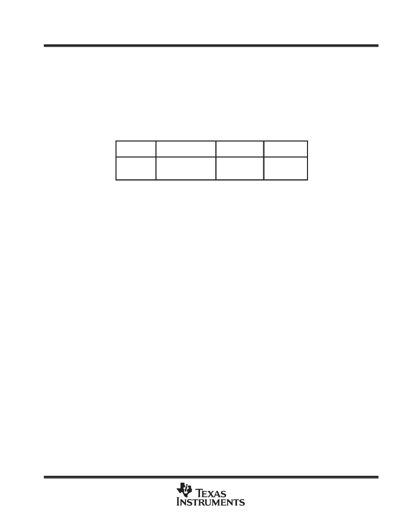
BIAS MODE
AC PERFORMANCE
BIAS SELECT
CONNECTION
TYPICAL IDD
Low
Medium
High
Low
Medium
High
VDD
0.8 V to 9.2 V
Ground pin
10
μ
A
150
μ
A
1000
μ
A
Bias selection may also be controlled by external circuitry to conserve power, etc.
For information regarding BIAS SELECT, see Figure 3 in the typical
characteristics curves.
For IDD characteristics at voltages other than 10 V, see Figure 4 in the typical
characteristics curves.
output stage considerations
The amplifier’s output stage consists of a source-follower-connected pullup transistor and an open-drain
pulldown transistor. The high-level output voltage (V
OH
) is virtually independent of the I
DD
selection and
increases with higher values of V
DD
and reduced output loading. The low-level output voltage (V
OL
) decreases
with reduced output current and higher input common-mode voltage. With no load, V
OL
is essentially equal to
the potential of V
DD–
/GND.
input offset nulling
The TLC251C series offers external offset null control. Nulling may be achieved by adjusting a 25-k
potentiometer connected between the offset null terminals with the wiper connected to the device V
DD–
/GND
pin as shown in Figure 2. The amount of nulling range varies with the bias selection. At an I
DD
setting of
1000
μ
A (high bias), the nulling range allows the maximum offset specified to be trimmed to zero. In low or
medium bias or when the amplifier is used below 4 V, total nulling may not be possible for all units.
supply configurations
Even though the TLC251C series is characterized for single-supply operation, it can be used effectively in a
split-supply configuration when the input common-mode voltage (V
ICR
), output swing (V
OL
and V
OH
), and
supply voltage limits are not exceeded.
circuit layout precautions
The user is cautioned that whenever extremely high circuit impedances are used, care must be exercised in
layout, construction, board cleanliness, and supply filtering to avoid hum and noise pickup, as well as excessive
dc leakages.
相關(guān)PDF資料 |
PDF描述 |
|---|---|
| TLC251Y | LinCMOSE PROGRAMMABLE LOW-POWER OPERATIONAL AMPLIFIERS |
| TLC2543C | 12-BIT ANALOG-TO-DIGITAL CONVERTERS WITH SERIAL CONTROL AND 11 ANALOG INPUTS |
| TLC2543I | 12-BIT ANALOG-TO-DIGITAL CONVERTERS WITH SERIAL CONTROL AND 11 ANALOG INPUTS |
| TLC2543MFK | 12-BIT ANALOG-TO-DIGITAL CONVERTERS WITH SERIAL CONTROL AND 11 ANALOG INPUTS |
| TLC2558CPW | BUTT SPLICE,NON-INS. RoHS Compliant: Yes |
相關(guān)代理商/技術(shù)參數(shù) |
參數(shù)描述 |
|---|---|
| TLC251BCP | 功能描述:運算放大器 - 運放 Programmable L RoHS:否 制造商:STMicroelectronics 通道數(shù)量:4 共模抑制比(最小值):63 dB 輸入補償電壓:1 mV 輸入偏流(最大值):10 pA 工作電源電壓:2.7 V to 5.5 V 安裝風(fēng)格:SMD/SMT 封裝 / 箱體:QFN-16 轉(zhuǎn)換速度:0.89 V/us 關(guān)閉:No 輸出電流:55 mA 最大工作溫度:+ 125 C 封裝:Reel |
| TLC251BCPE4 | 功能描述:運算放大器 - 運放 Programmable Lo-Pwr Op Amp RoHS:否 制造商:STMicroelectronics 通道數(shù)量:4 共模抑制比(最小值):63 dB 輸入補償電壓:1 mV 輸入偏流(最大值):10 pA 工作電源電壓:2.7 V to 5.5 V 安裝風(fēng)格:SMD/SMT 封裝 / 箱體:QFN-16 轉(zhuǎn)換速度:0.89 V/us 關(guān)閉:No 輸出電流:55 mA 最大工作溫度:+ 125 C 封裝:Reel |
| TLC251CD | 功能描述:運算放大器 - 運放 Programmable RoHS:否 制造商:STMicroelectronics 通道數(shù)量:4 共模抑制比(最小值):63 dB 輸入補償電壓:1 mV 輸入偏流(最大值):10 pA 工作電源電壓:2.7 V to 5.5 V 安裝風(fēng)格:SMD/SMT 封裝 / 箱體:QFN-16 轉(zhuǎn)換速度:0.89 V/us 關(guān)閉:No 輸出電流:55 mA 最大工作溫度:+ 125 C 封裝:Reel |
| TLC251CDG4 | 功能描述:運算放大器 - 運放 LinCMOS Prog Low-Power RoHS:否 制造商:STMicroelectronics 通道數(shù)量:4 共模抑制比(最小值):63 dB 輸入補償電壓:1 mV 輸入偏流(最大值):10 pA 工作電源電壓:2.7 V to 5.5 V 安裝風(fēng)格:SMD/SMT 封裝 / 箱體:QFN-16 轉(zhuǎn)換速度:0.89 V/us 關(guān)閉:No 輸出電流:55 mA 最大工作溫度:+ 125 C 封裝:Reel |
| TLC251CDR | 功能描述:運算放大器 - 運放 LinCMOS Prog Low-Power RoHS:否 制造商:STMicroelectronics 通道數(shù)量:4 共模抑制比(最小值):63 dB 輸入補償電壓:1 mV 輸入偏流(最大值):10 pA 工作電源電壓:2.7 V to 5.5 V 安裝風(fēng)格:SMD/SMT 封裝 / 箱體:QFN-16 轉(zhuǎn)換速度:0.89 V/us 關(guān)閉:No 輸出電流:55 mA 最大工作溫度:+ 125 C 封裝:Reel |
發(fā)布緊急采購,3分鐘左右您將得到回復(fù)。