- 您現(xiàn)在的位置:買賣IC網(wǎng) > PDF目錄383952 > TLC251Y (Texas Instruments, Inc.) LinCMOSE PROGRAMMABLE LOW-POWER OPERATIONAL AMPLIFIERS PDF資料下載
參數(shù)資料
| 型號(hào): | TLC251Y |
| 廠商: | Texas Instruments, Inc. |
| 英文描述: | LinCMOSE PROGRAMMABLE LOW-POWER OPERATIONAL AMPLIFIERS |
| 中文描述: | LinCMOSE可編程低功耗運(yùn)算放大器 |
| 文件頁數(shù): | 1/18頁 |
| 文件大小: | 273K |
| 代理商: | TLC251Y |
TLC251, TLC251A, TLC251B, TLC251Y
LinCMOS
PROGRAMMABLE
LOW-POWER OPERATIONAL AMPLIFIERS
SLOS001E – JULY 1983 – REVISED AUGUST 1994
1
POST OFFICE BOX 655303
DALLAS, TEXAS 75265
Wide Range of Supply Voltages
1.4 V to 16 V
True Single-Supply Operation
Common-Mode Input Voltage Range
Includes the Negative Rail
Low Noise . . . 30 nV/
√
Hz Typ at 1 kHz
(High Bias)
ESD Protection Exceeds 2000 V Per
MIL-STD-833C, Method 3015.1
description
The TLC251C, TLC251AC, and TLC251BC are
low-cost, low-power programmable operational
amplifiers designed to operate with single or dual
supplies. Unlike traditional metal-gate CMOS
operational amplifiers, these devices utilize Texas
Instruments silicon-gate LinCMOS
process,
giving them stable input offset voltages without
sacrificing the advantages of metal-gate CMOS.
This series of parts is available in selected grades of input offset voltage and can be nulled with one external
potentiometer. Because the input common-mode range extends to the negative rail and the power consumption
is extremely low, this family is ideally suited for battery-powered or energy-conserving applications. A
bias-select pin can be used to program one of three ac performance and power-dissipation levels to suit the
application. The series features operation down to a 1.4-V supply and is stable at unity gain.
These devices have internal electrostatic-discharge (ESD) protection circuits that prevent catastrophic failures
at voltages up to 2000 V as tested under MIL-STD-883C, Method 3015.1. However, care should be exercised
in handling these devices as exposure to ESD may result in a degradation of the device parametric
performance.
Because of the extremely high input impedance and low input bias and offset currents, applications for the
TLC251C series include many areas that have previously been limited to BIFET and NFET product types. Any
circuit using high-impedance elements and requiring small offset errors is a good candidate for cost-effective
use of these devices. Many features associated with bipolar technology are available with LinCMOS
operational amplifiers without the power penalties of traditional bipolar devices. Remote and inaccessible
equipment applications are possible using the low-voltage and low-power capabilities of the TLC251C series.
In addition, by driving the bias-select input with a logic signal from a microprocessor, these operational amplifiers
can have software-controlled performance and power consumption. The TLC251C series is well suited to solve
the difficult problems associated with single battery and solar cell-powered applications.
The TLC251C series is characterized for operation from 0
°
C to 70
°
C.
AVAILABLE OPTIONS
VIOmax
AT 25
°
C
PACKAGED DEVICES
SMALL OUTLINE
(D)
CHIP FORM
(Y)
TA
PLASTIC DIP
(P)
10 mV
5 mV
2 mV
TLC251CD
TLC251ACD
TLC251BCD
TLC251CP
TLC251ACP
TLC251BCP
TLC251Y
—
—
0
°
C to 70
°
C
The D package is available taped and reeled. Add the suffix R to the device type (e.g., TLC251CDR). Chips are
tested at 25
°
C.
Copyright
1994, Texas Instruments Incorporated
PRODUCTION DATA information is current as of publication date.
Products conform to specifications per the terms of Texas Instruments
standard warranty. Production processing does not necessarily include
testing of all parameters.
LinCMOS is a trademark of Texas Instruments Incorporated.
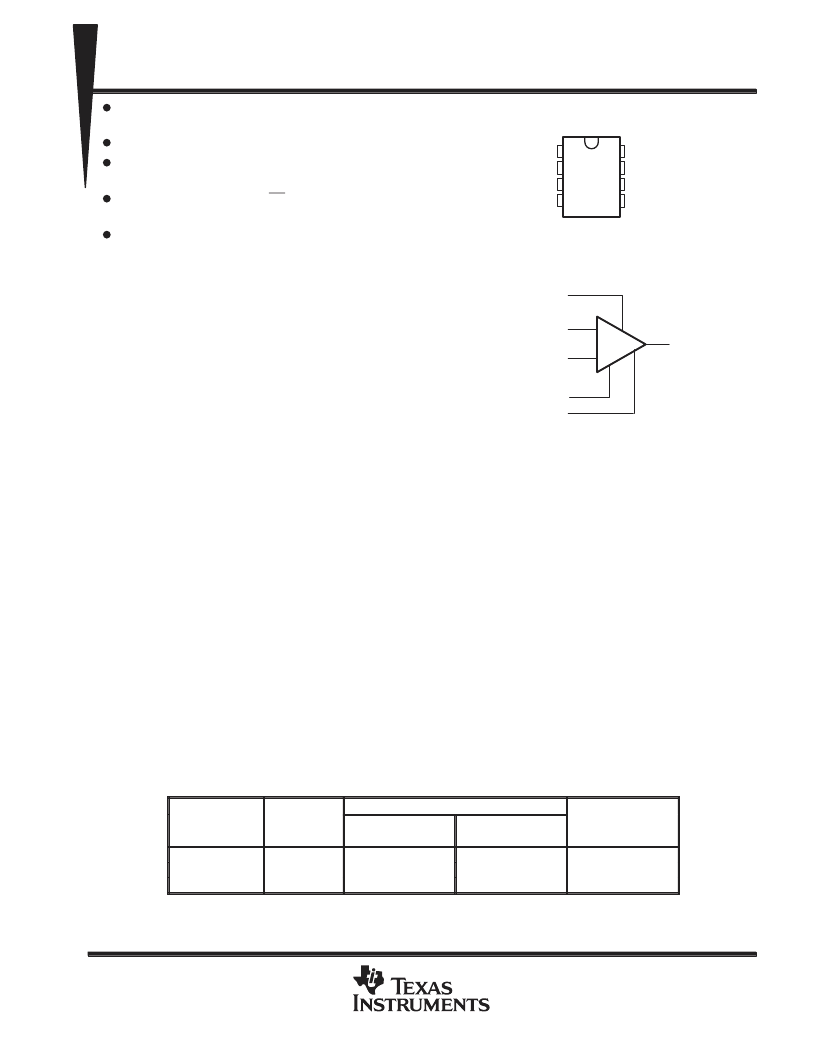
1
2
3
4
8
7
6
5
OFFSET N1
IN–
IN+
V
DD–
/GND
BIAS SELECT
V
DD
OUT
OFFSET N2
D OR P PACKAGE
(TOP VIEW)
symbol
+
–
OUT
BIAS SELECT
IN+
IN–
OFFSET N1
OFFSET N2
相關(guān)PDF資料 |
PDF描述 |
|---|---|
| TLC2543C | 12-BIT ANALOG-TO-DIGITAL CONVERTERS WITH SERIAL CONTROL AND 11 ANALOG INPUTS |
| TLC2543I | 12-BIT ANALOG-TO-DIGITAL CONVERTERS WITH SERIAL CONTROL AND 11 ANALOG INPUTS |
| TLC2543MFK | 12-BIT ANALOG-TO-DIGITAL CONVERTERS WITH SERIAL CONTROL AND 11 ANALOG INPUTS |
| TLC2558CPW | BUTT SPLICE,NON-INS. RoHS Compliant: Yes |
| TLC2554CPW | 5-V, 12-BIT, 400 KSPS, 4/8 CHANNEL, LOW POWER, SERIAL ANALOG-TO-DIGITAL CONVERTERS WITH AUTO POWER DOWN |
相關(guān)代理商/技術(shù)參數(shù) |
參數(shù)描述 |
|---|---|
| TLC252ACD | 功能描述:運(yùn)算放大器 - 運(yùn)放 Dual Low Power RoHS:否 制造商:STMicroelectronics 通道數(shù)量:4 共模抑制比(最小值):63 dB 輸入補(bǔ)償電壓:1 mV 輸入偏流(最大值):10 pA 工作電源電壓:2.7 V to 5.5 V 安裝風(fēng)格:SMD/SMT 封裝 / 箱體:QFN-16 轉(zhuǎn)換速度:0.89 V/us 關(guān)閉:No 輸出電流:55 mA 最大工作溫度:+ 125 C 封裝:Reel |
| TLC252ACDG4 | 功能描述:運(yùn)算放大器 - 運(yùn)放 LinCMOS Dual OP AMP RoHS:否 制造商:STMicroelectronics 通道數(shù)量:4 共模抑制比(最小值):63 dB 輸入補(bǔ)償電壓:1 mV 輸入偏流(最大值):10 pA 工作電源電壓:2.7 V to 5.5 V 安裝風(fēng)格:SMD/SMT 封裝 / 箱體:QFN-16 轉(zhuǎn)換速度:0.89 V/us 關(guān)閉:No 輸出電流:55 mA 最大工作溫度:+ 125 C 封裝:Reel |
| TLC252BCD | 功能描述:運(yùn)算放大器 - 運(yùn)放 Dual Low Power RoHS:否 制造商:STMicroelectronics 通道數(shù)量:4 共模抑制比(最小值):63 dB 輸入補(bǔ)償電壓:1 mV 輸入偏流(最大值):10 pA 工作電源電壓:2.7 V to 5.5 V 安裝風(fēng)格:SMD/SMT 封裝 / 箱體:QFN-16 轉(zhuǎn)換速度:0.89 V/us 關(guān)閉:No 輸出電流:55 mA 最大工作溫度:+ 125 C 封裝:Reel |
| TLC252BCDG4 | 功能描述:運(yùn)算放大器 - 運(yùn)放 LinCMOS Dual Op Amp RoHS:否 制造商:STMicroelectronics 通道數(shù)量:4 共模抑制比(最小值):63 dB 輸入補(bǔ)償電壓:1 mV 輸入偏流(最大值):10 pA 工作電源電壓:2.7 V to 5.5 V 安裝風(fēng)格:SMD/SMT 封裝 / 箱體:QFN-16 轉(zhuǎn)換速度:0.89 V/us 關(guān)閉:No 輸出電流:55 mA 最大工作溫度:+ 125 C 封裝:Reel |
| TLC252BCDR | 功能描述:運(yùn)算放大器 - 運(yùn)放 LinCMOS Dual Op Amp RoHS:否 制造商:STMicroelectronics 通道數(shù)量:4 共模抑制比(最小值):63 dB 輸入補(bǔ)償電壓:1 mV 輸入偏流(最大值):10 pA 工作電源電壓:2.7 V to 5.5 V 安裝風(fēng)格:SMD/SMT 封裝 / 箱體:QFN-16 轉(zhuǎn)換速度:0.89 V/us 關(guān)閉:No 輸出電流:55 mA 最大工作溫度:+ 125 C 封裝:Reel |
發(fā)布緊急采購,3分鐘左右您將得到回復(fù)。