- 您現(xiàn)在的位置:買賣IC網(wǎng) > PDF目錄383949 > TL16C550 (Texas Instruments, Inc.) ASYNCHRONOUS COMMUNICATIONS ELEMENT PDF資料下載
參數(shù)資料
| 型號: | TL16C550 |
| 廠商: | Texas Instruments, Inc. |
| 英文描述: | ASYNCHRONOUS COMMUNICATIONS ELEMENT |
| 中文描述: | 異步通信元 |
| 文件頁數(shù): | 8/35頁 |
| 文件大?。?/td> | 499K |
| 代理商: | TL16C550 |
第1頁第2頁第3頁第4頁第5頁第6頁第7頁當前第8頁第9頁第10頁第11頁第12頁第13頁第14頁第15頁第16頁第17頁第18頁第19頁第20頁第21頁第22頁第23頁第24頁第25頁第26頁第27頁第28頁第29頁第30頁第31頁第32頁第33頁第34頁第35頁
TL16C550B, TL16C550BI
ASYNCHRONOUS COMMUNICATIONS ELEMENT
SLLS136B – JANUARY 1994 – REVISED AUGUST 1996
8
POST OFFICE BOX 655303
DALLAS, TEXAS 75265
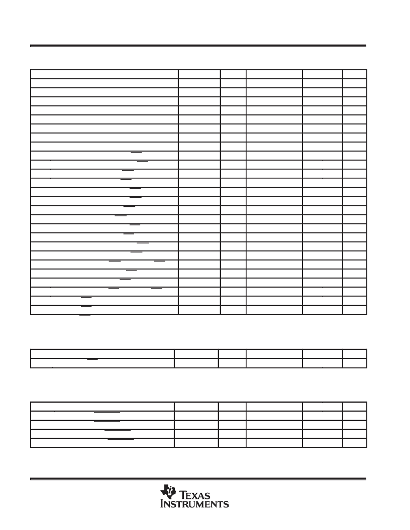
system timing requirements over recommended ranges of supply voltage and operating free-air
temperature
PARAMETER
ALT. SYMBOL
FIGURE
TEST CONDITIONS
MIN
MAX
UNIT
tcR
tcW
tw1
tw2
tw5
tw6
tw7
tw8
tsu1
tsu2
tsu3
th1
th2
th3
th4
th5
th6
th7
td4
td5
td6
td7
td8
td9
td10
td11
Only applies when ADS is low
Cycle time, read (tw7 + td8 + td9)
Cycle time, write (tw6 + td5 + td6)
Pulse duration, clock high
RC
87
ns
WC
87
ns
tXH
tXL
tADS
tWR
tRD
1
f = 9 MHz maximum
40
ns
Pulse duration, clock low
1
f = 9 MHz maximum
40
ns
Pulse duration, address strobe low
2,3
9
ns
Pulse duration, write strobe
2
40
ns
Pulse duration, read strobe
3
40
ns
μ
s
ns
Pulse duration, master reset
Setup time, address valid before ADS
↑
Setup time, chip select valid before ADS
↑
Setup time, data valid before WR1
↓
or WR2
↑
Hold time, address low after ADS
↑
Hold time, chip select valid after ADS
↑
Hold time, chip select valid after WR1
↑
or WR2
↓
Hold time, address valid after WR1
↑
or WR2
↓
Hold time, data valid after WR1
↑
or WR2
↓
Hold time, chip select valid after RD1
↑
or RD2
↓
Hold time, address valid after RD1
↑
or RD2
↓
Delay time, chip select valid before WR1
↓
or WR2
↑
Delay time, address valid before WR1
↓
or WR2
↑
Delay time, write cycle, WR1
↑
or WR2
↓
to ADS
↓
Delay time, chip select valid to RD1
↓
or RD2
↑
Delay time, address valid to RD1
↓
or RD2
↑
Delay time, read cycle, RD1
↑
or RD2
↓
to ADS
↓
Delay time, RD1
↓
or RD2
↑
to data valid
Delay time, RD1
↑
or RD2
↓
to floating data
tMR
tAS
tCS
tDS
tAH
tCH
tWCS
tWA
tDH
tRCS
tRA
tCSW
tAW
tWC
tCSR
tAR
tRC
1
2,3
8
2,3
8
ns
2
15
ns
2,3
0
ns
2,3
0
ns
2
10
ns
2
10
ns
2
5
ns
3
10
ns
3
20
ns
2
7
ns
2
7
ns
2
40
ns
3
7
ns
3
7
ns
3
40
ns
tRVD
tHZ
3
CL = 75 pF
CL = 75 pF
45
ns
3
20
ns
system switching characteristics over recommended ranges of supply voltage and operating
free-air temperature (see Note 2)
PARAMETER
ALT. SYMBOL
FIGURE
TEST CONDITIONS
MIN
MAX
UNIT
tdis(R)
NOTE 2: Charge and discharge time is determined by VOL, VOH, and external loading.
Disable time, RD1
↑↓
or RD2
↓↑
to DDIS
↑↓
tRDD
3
CL = 75 pF
20
ns
baud generator switching characteristics over recommended ranges of supply voltage and
operating free-air temperature, C
L
= 75 pF
PARAMETER
ALT. SYMBOL
FIGURE
TEST CONDITIONS
f = 9 MHz, CLK
÷
2
f = 9 MHz, CLK
÷
2
MIN
MAX
UNIT
tw3
tw4
td1
td2
Pulse duration, BAUDOUT low
tLW
tHW
tBLD
tBHD
1
80
ns
Pulse duration, BAUDOUT high
Delay time, XIN
↑
to BAUDOUT
↑
Delay time, XIN
↑↓
to BAUDOUT
↓
1
80
ns
1
75
ns
1
65
ns
相關(guān)PDF資料 |
PDF描述 |
|---|---|
| TL16C550BIN | ASYNCHRONOUS COMMUNICATIONS ELEMENT |
| TL16C550CIN | ASYNCHRONOUS COMMUNICATIONS ELEMENT WITH AUTOFLOW CONTROL |
| TL16C550CIPFB | ASYNCHRONOUS COMMUNICATIONS ELEMENT WITH AUTOFLOW CONTROL |
| TL16C552AMPN | DUAL ASYNCHRONOUS COMMUNICATIONS ELEMENT WITH FIFO |
| TL16C552AHV | DUAL ASYNCHRONOUS COMMUNICATIONS ELEMENT WITH FIFO |
相關(guān)代理商/技術(shù)參數(shù) |
參數(shù)描述 |
|---|---|
| TL16C550A | 制造商:TI 制造商全稱:Texas Instruments 功能描述:ASYNCHRONOUS COMMUNICATIONS ELEMENT |
| TL16C550AFN | 制造商:Rochester Electronics LLC 功能描述:- Bulk |
| TL16C550AN | 制造商:Rochester Electronics LLC 功能描述:- Bulk 制造商:Texas Instruments 功能描述: |
| TL16C550B | 制造商:TI 制造商全稱:Texas Instruments 功能描述:ASYNCHRONOUS COMMUNICATIONS ELEMENT WITH AUTOFLOW CONTROL |
| TL16C550B1FN | 制造商:Texas Instruments 功能描述: |
發(fā)布緊急采購,3分鐘左右您將得到回復。