- 您現(xiàn)在的位置:買賣IC網(wǎng) > PDF目錄383949 > TL16C550 (Texas Instruments, Inc.) ASYNCHRONOUS COMMUNICATIONS ELEMENT PDF資料下載
參數(shù)資料
| 型號(hào): | TL16C550 |
| 廠商: | Texas Instruments, Inc. |
| 英文描述: | ASYNCHRONOUS COMMUNICATIONS ELEMENT |
| 中文描述: | 異步通信元 |
| 文件頁數(shù): | 6/35頁 |
| 文件大小: | 499K |
| 代理商: | TL16C550 |
第1頁第2頁第3頁第4頁第5頁當(dāng)前第6頁第7頁第8頁第9頁第10頁第11頁第12頁第13頁第14頁第15頁第16頁第17頁第18頁第19頁第20頁第21頁第22頁第23頁第24頁第25頁第26頁第27頁第28頁第29頁第30頁第31頁第32頁第33頁第34頁第35頁
TL16C550B, TL16C550BI
ASYNCHRONOUS COMMUNICATIONS ELEMENT
SLLS136B – JANUARY 1994 – REVISED AUGUST 1996
6
POST OFFICE BOX 655303
DALLAS, TEXAS 75265
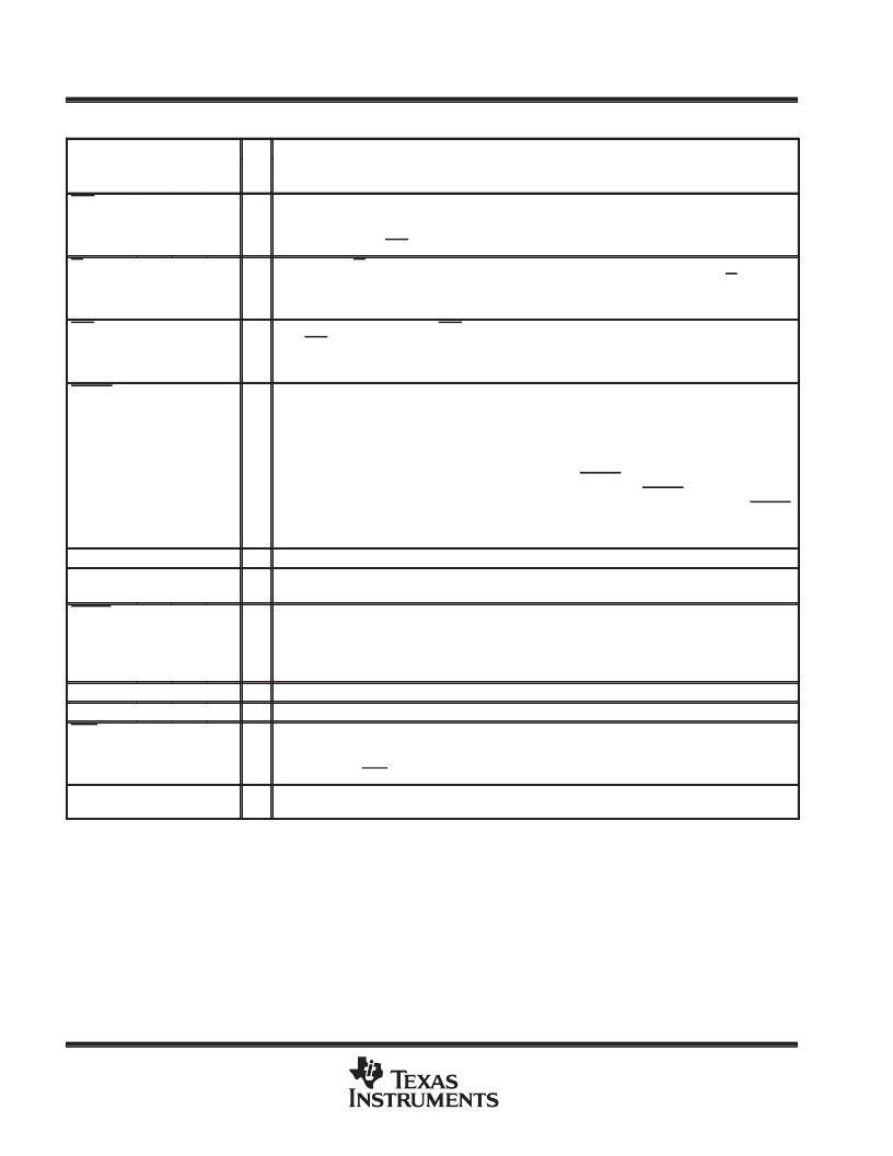
Terminal Functions (Continued)
TERMINAL
NO.
N
NAME
NO.
FN
NO.
PT
I/O
DESCRIPTION
RD1
RD2
21
22
24
25
19
20
I
Read inputs. When either input is active (low or high respectively) while the ACE is selected, the CPU
is allowed to read status information or data from a selected ACE register. Only one of these inputs is
required for the transfer of data during a read operation; the other input should be tied in its inactive state
(i.e., RD2 tied low or RD1 tied high).
RI
39
43
41
I
Ring indicator. RI is a modem status signal. Its condition can be checked by reading bit 6 (RI) of the
modem status register. Bit 2 (TERI) of the modem status register indicates that the RI input has
transitioned from a low to a high state since the last read from the modem status register. If the modem
status interrupt is enabled when this transition occurs, an interrupt is generated.
RTS
32
36
32
O
Request to send. When active, RTS informs the modem or data set that the ACE is ready to receive
data. RTS is set to its active state by setting the RTS modem control register bit and is set to its inactive
(high) state either as a result of a master reset or during loop mode operations or by clearing bit 1 (RTS)
of the MCR.
RXRDY
29
32
29
O
Receiver ready output. Receiver direct memory access (DMA) signalling is available with this terminal.
When operating in the FIFO mode, one of two types of DMA signalling can be selected using the FIFO
control register bit 3 (FCR3). When operating in the TL16C450 mode, only DMA mode 0 is allowed.
Mode 0 supports single-transfer DMA in which a transfer is made between CPU bus cycles. Mode 1
supports multitransfer DMA in which multiple transfers are made continuously until the receiver FIFO
has been emptied. In DMA mode 0 (FCR0 = 0 or FCR0 = 1, FCR3 = 0), when there is at least one
character in the receiver FIFO or receiver holding register, RXRDY is active low. When RXRDY has
been active but there are no characters in the FIFO or holding register, RXRDY goes inactive (high).
In DMA mode 1 (FCR0 = 1, FCR3 = 1), when the trigger level or the timeout has been reached, RXRDY
goes active (low); when it has been active but there are no more characters in the FIFO or holding
register, it goes inactive (high).
SIN
10
11
7
I
Serial data input. Input from a connected communications device
SOUT
11
13
8
O
Composite serial data output. Output to a connected communication device. SOUT is set to the marking
(set) state as a result of master reset.
TXRDY
24
27
23
O
Transmitter ready output. Transmitter DMA signalling is available with this terminal. When operating in
the FIFO mode, one of two types of DMA signalling can be selected using FCR3. When operating in
the TL16C450 mode, only DMA mode 0 is allowed. Mode 0 supports single-transfer DMA in which a
transfer is made between CPU bus cycles. Mode 1 supports multitransfer DMA in which multiple
transfers are made continuously until the transmit FIFO has been filled.
VCC
VSS
WR1
WR2
40
44
42
5-V supply voltage
20
22
18
Supply common
18
19
20
21
16
17
I
Write inputs. When either input is active (high or low respectively) and while the ACE is selected, the
CPU is allowed to write control words or data into a selected ACE register. Only one of these inputs is
required to transfer data during a write operation; the other input should be tied in its inactive state (i.e.,
WR2 tied low or WR1 tied high).
XIN
XOUT
16
17
18
19
14
15
I/O
External clock. XIN and XOUT connect the ACE to the main timing reference (clock or crystal).
相關(guān)PDF資料 |
PDF描述 |
|---|---|
| TL16C550BIN | ASYNCHRONOUS COMMUNICATIONS ELEMENT |
| TL16C550CIN | ASYNCHRONOUS COMMUNICATIONS ELEMENT WITH AUTOFLOW CONTROL |
| TL16C550CIPFB | ASYNCHRONOUS COMMUNICATIONS ELEMENT WITH AUTOFLOW CONTROL |
| TL16C552AMPN | DUAL ASYNCHRONOUS COMMUNICATIONS ELEMENT WITH FIFO |
| TL16C552AHV | DUAL ASYNCHRONOUS COMMUNICATIONS ELEMENT WITH FIFO |
相關(guān)代理商/技術(shù)參數(shù) |
參數(shù)描述 |
|---|---|
| TL16C550A | 制造商:TI 制造商全稱:Texas Instruments 功能描述:ASYNCHRONOUS COMMUNICATIONS ELEMENT |
| TL16C550AFN | 制造商:Rochester Electronics LLC 功能描述:- Bulk |
| TL16C550AN | 制造商:Rochester Electronics LLC 功能描述:- Bulk 制造商:Texas Instruments 功能描述: |
| TL16C550B | 制造商:TI 制造商全稱:Texas Instruments 功能描述:ASYNCHRONOUS COMMUNICATIONS ELEMENT WITH AUTOFLOW CONTROL |
| TL16C550B1FN | 制造商:Texas Instruments 功能描述: |
發(fā)布緊急采購,3分鐘左右您將得到回復(fù)。