- 您現(xiàn)在的位置:買賣IC網(wǎng) > PDF目錄383949 > TL1591CPS (Texas Instruments, Inc.) 192- 】 165-pixel ccd image sensor PDF資料下載
參數(shù)資料
| 型號: | TL1591CPS |
| 廠商: | Texas Instruments, Inc. |
| 英文描述: | 192- 】 165-pixel ccd image sensor |
| 中文描述: | 192 - 】165萬像素CCD圖像傳感器 |
| 文件頁數(shù): | 2/13頁 |
| 文件大?。?/td> | 173K |
| 代理商: | TL1591CPS |
TC211
192-
×
165-PIXEL CCD IMAGE SENSOR
SOCS008B – JANUARY 1990
2-2
POST OFFICE BOX 655303
DALLAS, TEXAS 75265
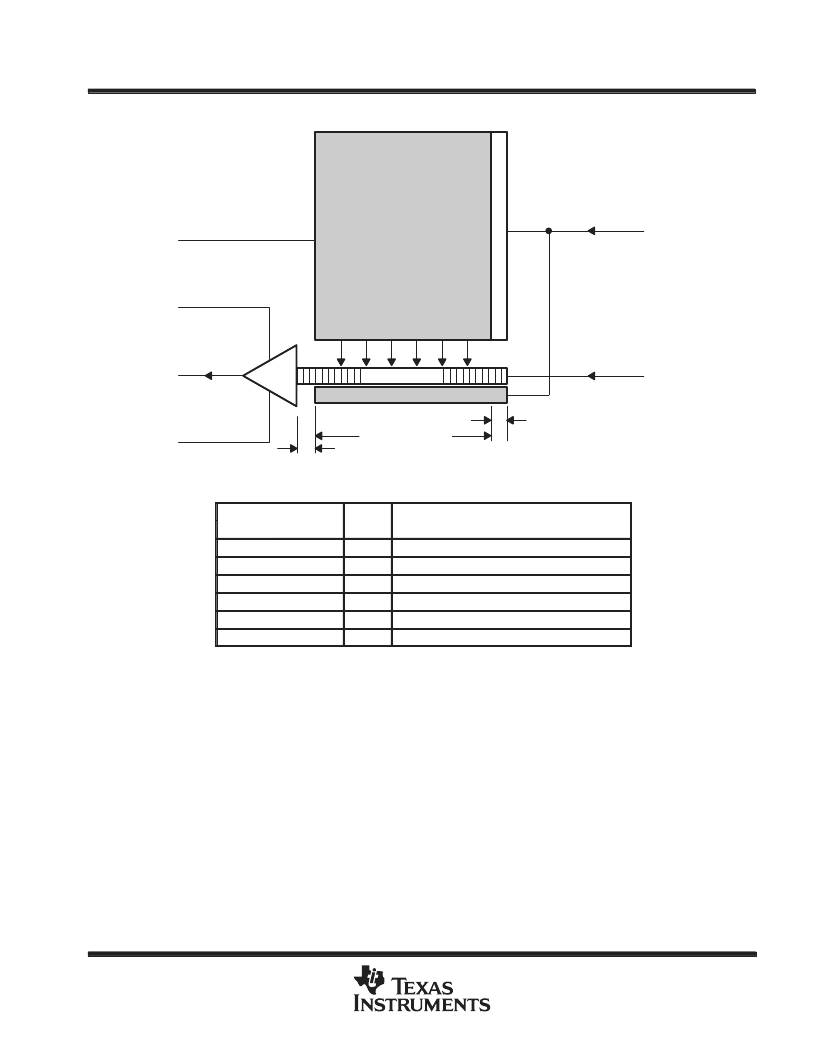
functional block diagram
Serial Register
1
192
Clear Gate
165
12 Dark Pixels
192 Image Pixels
6 Dummy Pixels
ABG
ADB
OUT
VSS
1
3
4
2
6
5
1
IAG
SRG
Terminal Functions
TERMINAL
I/O
DESCRIPTION
NAME
ABG
NO.
1
I
Antiblooming gate
VSS
ADB
2
Amplifier ground
3
I
Supply voltage for amplifier drain bias
OUT
4
O
Output signal
SRG
5
I
Serial-register gate
IAG
6
I
Image-area gate storage
functional description
The image-sensing area consists of 165 horizontal image lines each containing 192 photosensitive elements
(pixels). Each pixel is 13.75
μ
m (horizontal) by 16.00
μ
m (vertical). As light enters the silicon in the
image-sensing area, free electrons are generated and collected in potential wells (see Figure 1). During this
time, the antiblooming gate is activated by applying a burst of pulses every horizontal blanking interval. This
prevents blooming caused by the spilling of charge from overexposed elements into neighboring elements. The
antiblooming gate is typically held at a midlevel voltage during readout. The quantity of charge collected in each
pixel is a linear function of the incident light and the exposure time. After exposure and under dark conditions,
the charge packets are transferred from the image area to the serial register at the rate of one image line per
each clock pulse applied to the image-area gate. Once an image line has been transferred into the serial register,
the serial-register gate can be clocked until all of the charge packets are moved out of the serial register to the
charge detection node at the amplifier input.
There are 12 dark pixels to the right of the 192 image pixels on each image line. These dark pixels are shielded
from incident light and the signal derived from them can be used to generate a dark reference for restoration
of the video black level on the next image line.
相關(guān)PDF資料 |
PDF描述 |
|---|---|
| TL16C550BI | ASYNCHRONOUS COMMUNICATIONS ELEMENT |
| TL16C550 | ASYNCHRONOUS COMMUNICATIONS ELEMENT |
| TL16C550BIN | ASYNCHRONOUS COMMUNICATIONS ELEMENT |
| TL16C550CIN | ASYNCHRONOUS COMMUNICATIONS ELEMENT WITH AUTOFLOW CONTROL |
| TL16C550CIPFB | ASYNCHRONOUS COMMUNICATIONS ELEMENT WITH AUTOFLOW CONTROL |
相關(guān)代理商/技術(shù)參數(shù) |
參數(shù)描述 |
|---|---|
| TL1591CPSLE | 制造商:TI 制造商全稱:Texas Instruments 功能描述:SAMPLE-AND-HOLD CIRCUIT FOR CCD IMAGERS |
| TL1593 | 制造商:TI 制造商全稱:Texas Instruments 功能描述:3-CHANNEL SAMPLE-AND-HOLD CIRCUIT |
| TL1593C | 制造商:TI 制造商全稱:Texas Instruments 功能描述:3-CHANNEL SAMPLE-AND-HOLD CIRCUIT |
| TL1593CNS | 制造商:TI 制造商全稱:Texas Instruments 功能描述:3-CHANNEL SAMPLE-AND-HOLD CIRCUIT |
| TL159A-E-W1 | 制造商:Black Box Corporation 功能描述:1 year warranty for TL159A-E |
發(fā)布緊急采購,3分鐘左右您將得到回復(fù)。