- 您現(xiàn)在的位置:買賣IC網(wǎng) > PDF目錄98229 > THS8083APZPG4 (TEXAS INSTRUMENTS INC) SPECIALTY CONSUMER CIRCUIT, PQFP100 PDF資料下載
參數(shù)資料
| 型號: | THS8083APZPG4 |
| 廠商: | TEXAS INSTRUMENTS INC |
| 元件分類: | 消費家電 |
| 英文描述: | SPECIALTY CONSUMER CIRCUIT, PQFP100 |
| 封裝: | GREEN, PLASTIC, HTQFP-100 |
| 文件頁數(shù): | 7/63頁 |
| 文件大小: | 320K |
| 代理商: | THS8083APZPG4 |
第1頁第2頁第3頁第4頁第5頁第6頁當(dāng)前第7頁第8頁第9頁第10頁第11頁第12頁第13頁第14頁第15頁第16頁第17頁第18頁第19頁第20頁第21頁第22頁第23頁第24頁第25頁第26頁第27頁第28頁第29頁第30頁第31頁第32頁第33頁第34頁第35頁第36頁第37頁第38頁第39頁第40頁第41頁第42頁第43頁第44頁第45頁第46頁第47頁第48頁第49頁第50頁第51頁第52頁第53頁第54頁第55頁第56頁第57頁第58頁第59頁第60頁第61頁第62頁第63頁

32
In the case of YUV input signals, blanking levels for U and V correspond to the mid-level analog input. To handle these
signals the clamping range should be centered on the mid-level output code of the A/D.
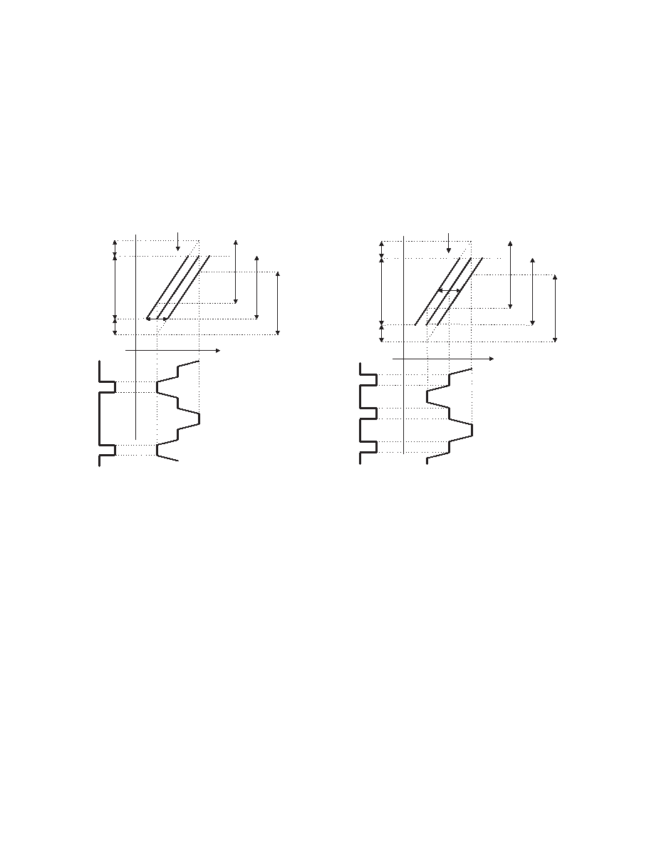
The clamp code is 8 bits wide and spans 128 ADC output codes (a 2 LSB change to clamp code corresponds
nominally to 1 LSB change in ADC output). The programmed clamp code is independent of the PGA setting (see
later). This ensures independent brightness/clamping control.
The clamp pulse defines the timing window during which the clamp circuit is internally enabled, and is either generated
externally and supplied to the device, or it can be internally generated. In the latter case, the user can program both
the position and width of the clamp pulse with respect to the horizontal sync (HS) input.
0
255
CLIP 255
CLIP 0
+63
64
0
CLAMP CODE
ADC Output
Code Range
VIN
CLP PULSE
63
= +63 = 0
191
= 64
0
255
CLIP 255
CLIP 0
+63
64
0
CLAMP CODE
ADC Output
Code Range
VIN
CLP PULSE
63
= +63
= 0
191
= 64
Figure 32. Bottom-Level Clamping
Figure 33. Mid-Level Clamping
Influence of changing clamp codes on
A/D output, while keeping PGA gain setting
constant, in bottom-level clamp mode
Influence of changing clamp codes on
A/D output, while keeping PGA gain setting
constant, in midlevel clamp mode
3.3
Composite Sync Slicer
The THS8083A includes a circuit that compares the input signal on Ch.1, or on the dedicated CS_IN input, to a level
150 mV below the blanking level. This slicer outputs a 3-V compatible digital output on the composite sync (CS) pin.
The intended use of this circuit is for input video signals that have an embedded (negative or trilevel) sync. This is
the case for workstation-type input signals or the DTV analog interface that mandates sync-on-Y. Since the sync
amplitude is ~300 mV, the slicing level is at about 50% of the sync level. When enabled, the CS output is available
even when the device is powered down.
CS outputs the extracted composite sync. Since the PLL is prevented from updating its phase detector while the
PFD_FREEZE pin is kept high, the user asserts PFD_FREEZE during the VBI (when CS has multiple transitions per
line). This puts the PLL in free-run. While it cannot be assured with devices that have analog PLL’s, the digital PLL
in the THS8083A is assured to keep a constant output frequency and avoid frequency drift while the PLL is in free-run.
There is also no maximum on the time that PFD_FREEZE can be kept asserted to still keep a stable PLL output
frequency. In this case, the CS output can be directly connected to the THS8083A’s HS input for purposes of locking
the PLL. However, the frequency monitoring of HS, which works off signal edges, produces invalid numbers on those
lines where CS is present because of the multiple low-high transitions on these lines.
相關(guān)PDF資料 |
PDF描述 |
|---|---|
| THS8083CPZP | SPECIALTY CONSUMER CIRCUIT, PQFP100 |
| THS8133ACPHP | PARALLEL, WORD INPUT LOADING, 0.005 us SETTLING TIME, 10-BIT DAC, PQFP48 |
| THS8133BCPHP | PARALLEL, WORD INPUT LOADING, 0.005 us SETTLING TIME, 10-BIT DAC, PQFP48 |
| THS8133BCPHPG4 | PARALLEL, WORD INPUT LOADING, 0.005 us SETTLING TIME, 10-BIT DAC, PQFP48 |
| THS8133CPHP | PARALLEL, WORD INPUT LOADING, 0.005 us SETTLING TIME, 10-BIT DAC, PQFP48 |
相關(guān)代理商/技術(shù)參數(shù) |
參數(shù)描述 |
|---|---|
| THS8083CPZP | 制造商:Rochester Electronics LLC 功能描述:- Bulk |
| THS8083EVM | 制造商:Texas Instruments 功能描述:THS8083EVM - Bulk |
| THS8083T | 制造商:TI 制造商全稱:Texas Instruments 功能描述:Triple 8-Bit, 80 MSPS, 3.3-V Video and Graphics Digitizer With Digital PLL |
| THS8-10R-D | 制造商:Thomas & Betts 功能描述:CATAMOUNT CABLE TIES |
| THS8133 | 制造商:TI 制造商全稱:Texas Instruments 功能描述:TRIPLE 10-BIT, 80 MSPS VIDEO D/A CONVERTER WITH TRI-LEVEL SYNC GENERATION WITH TRI-LEVEL SYNC GENERATION |
發(fā)布緊急采購,3分鐘左右您將得到回復(fù)。