- 您現(xiàn)在的位置:買賣IC網(wǎng) > PDF目錄98229 > THS770012IRGET (TEXAS INSTRUMENTS INC) SPECIALTY ANALOG CIRCUIT, PQCC24 PDF資料下載
參數(shù)資料
| 型號: | THS770012IRGET |
| 廠商: | TEXAS INSTRUMENTS INC |
| 元件分類: | 模擬信號調(diào)理 |
| 英文描述: | SPECIALTY ANALOG CIRCUIT, PQCC24 |
| 封裝: | GREEN, PLASTIC, VQFN-24 |
| 文件頁數(shù): | 15/35頁 |
| 文件大?。?/td> | 1305K |
| 代理商: | THS770012IRGET |
第1頁第2頁第3頁第4頁第5頁第6頁第7頁第8頁第9頁第10頁第11頁第12頁第13頁第14頁當(dāng)前第15頁第16頁第17頁第18頁第19頁第20頁第21頁第22頁第23頁第24頁第25頁第26頁第27頁第28頁第29頁第30頁第31頁第32頁第33頁第34頁第35頁

V
ADC
REF
-
V
AMP
ADC
-
R
P
O
=R
GAIN=
2R ||Z
P
IN
2R +2R ||Z
O
P
IN
V
ADC FS
GAIN
V
AMP PP
=
SLOS669B
– FEBRUARY 2010 – REVISED MAY 2011
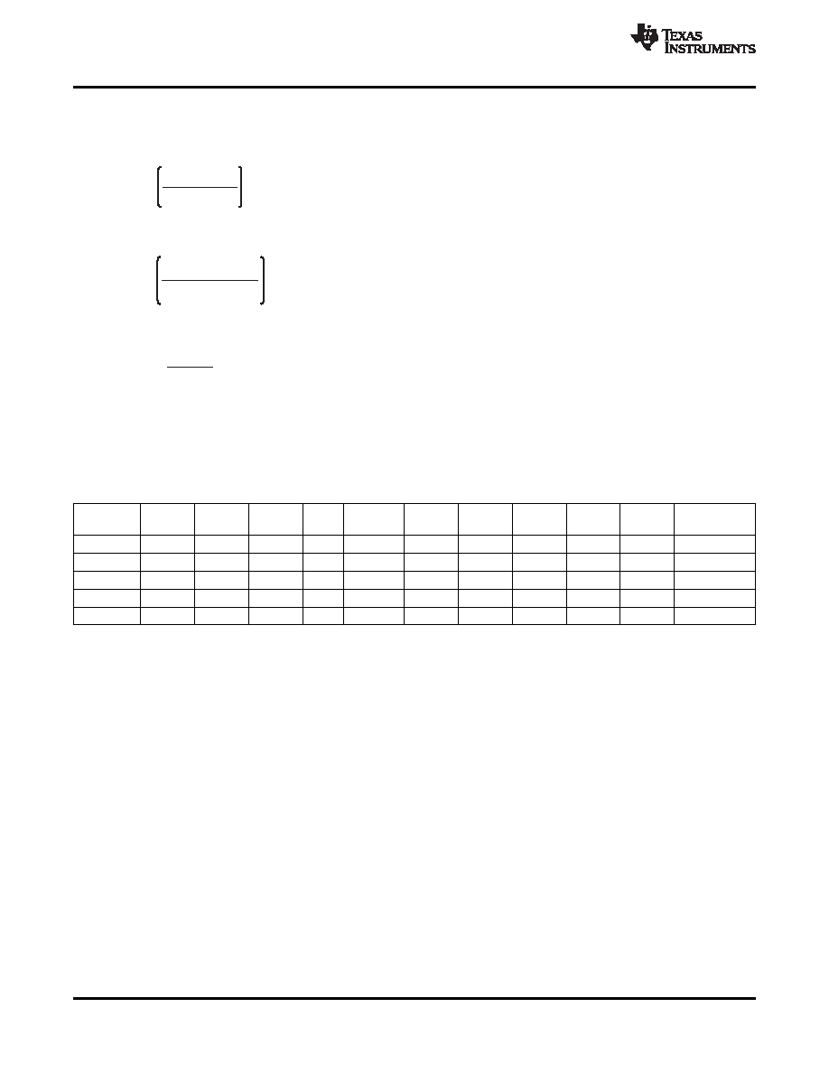
For common-mode analysis, assume that VAMP± = VOCM and VADC± = VADC (the specification for the ADC input
common-mode voltage). VREF is chosen to be a voltage within the system (such as the ADC or amplifier analog
supply) or ground, depending on whether the voltage must be pulled up or down, and RO is chosen to be a
reasonable value, such as 49.9
(1)
The insertion of this resistor network also attenuates the amplifier output signal. The gain (or loss) can be
calculated by Equation 2:
(2)
Using the gain and knowing the full-scale input of the ADC, VADC FS, the required amplitude to drive the ADC with
the network can be calculated using Equation 3:
(3)
Using the ADC examples given previously, Table 3 shows sample calculations of the value of RP and VAMP FS for
full-scale drive, and then for
–1dB (often times, the ADC drive is backed off from full-scale in applications, so
lower amplitudes may be acceptable). All voltages are in volts, resistors in
Ω (the nearest standard value should
be used), and gain as noted. Table 3 does not include the ADS5424 because no level shift is required with this
device.
Table 3. Example RP for Various ADCs
VOCM
VADC
VREF
RINT
RO
RP
GAIN
VADC FS
VAMP PP
ADC
(VDC)
(
Ω)
(
Ω)
(
Ω)
(V/V)
(dB)
(VPP)
FS (VPP)
–1dBFS (VPP)
ADS5485
2.5
3.1
5
1k
50
158.3
0.73
–2.71
2
4.10
3.65
ADS5493
2.5
3.15
5
1k
50
142.3
0.71
–2.93
2.5
3.50
3.12
ADS6149
2.5
1.5
0
NA
50
75.0
0.60
–4.44
2
3.33
2.97
ADS4149
2.5
0.95
0
NA
50
30.6
0.38
–8.40
2
5.26
4.69
ADS4149
0(1)
0.95
2.5
NA
50
81.6
0.62
–4.15
2
3.23
2.88
(1)
THS770012 with
±2.5V supply.
The calculated values for the ADS5485 give the lowest attenuation, and because of the high VFS, it requires
3.65VPP from the amplifier to drive to –1dBFS. Performance of the THS770012 is still very good up to 130MHz at
this level, but the designer may want to further back off from full-scale for best performance and consider trading
reduced SNR performance for better SFDR performance.
The calculated values for the ADS5493 have lower attenuation as a result of reduced VFS, and requires 3.12VPP
from the amplifier to drive to
–1dBFS. Performance of the THS770012 is excellent at this level up to 130MHz.
The values calculated for the ADS6149 show reasonable design targets and should work with good performance.
Note the ADS6149 does not have buffered inputs, and the inputs have equivalent resistive impedance that varies
with sampling frequency. In order to account for the increased loss, half of this resistance should be used for the
The values calculated for the low input common-mode of the ADS4149 result in large attenuation of the amplifier
signal leading to 5.26VPP being required for full-scale ADC drive. This amplitude is greater than the maximum
capability of the device. With a single +5V supply, the THS770012 is not suitable to drive this ADC in dc-coupled
applications unless the ADC input is backed off towards
–6dBFS. Another option is to operate the THS770012
with a split
±2.5V supply, and is shown in the last row of Table 3. For this situation, if the +2.5V is used as the
pull-up voltage, only 2.88VPP is required for the –1dBFS input to the ADS4149. See the Operation with Split
±2.5V section for more detail. Note that the ADS4149 does not have buffered inputs and the inputs have
equivalent resistive impedance that varies with sampling frequency. In order to account for the increased loss,
As with any design, testing is recommended to validate whether it meets the specific design goals.
22
Copyright
2010–2011, Texas Instruments Incorporated
相關(guān)PDF資料 |
PDF描述 |
|---|---|
| THS8083-95CPZP | SPECIALTY CONSUMER CIRCUIT, PQFP100 |
| THS8083APZP | SPECIALTY CONSUMER CIRCUIT, PQFP100 |
| THS8083APZPG4 | SPECIALTY CONSUMER CIRCUIT, PQFP100 |
| THS8083CPZP | SPECIALTY CONSUMER CIRCUIT, PQFP100 |
| THS8133ACPHP | PARALLEL, WORD INPUT LOADING, 0.005 us SETTLING TIME, 10-BIT DAC, PQFP48 |
相關(guān)代理商/技術(shù)參數(shù) |
參數(shù)描述 |
|---|---|
| THS788 | 制造商:TI 制造商全稱:Texas Instruments 功能描述:QUAD-CHANNEL TIME MEASUREMENT UNIT (TMU) |
| THS788PFD | 功能描述:計時器和支持產(chǎn)品 Quad Ch Time Msmt Unit RoHS:否 制造商:Micrel 類型:Standard 封裝 / 箱體:SOT-23 內(nèi)部定時器數(shù)量:1 電源電壓-最大:18 V 電源電壓-最小:2.7 V 最大功率耗散: 最大工作溫度:+ 85 C 最小工作溫度:- 40 C 封裝:Reel |
| THS788PFDT | 功能描述:計時器和支持產(chǎn)品 Quad Ch Time Msmt Unit RoHS:否 制造商:Micrel 類型:Standard 封裝 / 箱體:SOT-23 內(nèi)部定時器數(shù)量:1 電源電壓-最大:18 V 電源電壓-最小:2.7 V 最大功率耗散: 最大工作溫度:+ 85 C 最小工作溫度:- 40 C 封裝:Reel |
| THS789PFD | 制造商:Texas Instruments 功能描述:Time Measurement Unit (TMU) 100-Pin HTQFP EP Tray 制造商:Texas Instruments 功能描述:IC TIME MEASUREMNT UNIT 100HTQFP 制造商:Texas Instruments 功能描述:THS789PFD |
| THS7BAT | 功能描述:電池組 Rechargeable NICD For THS700 series RoHS:否 制造商:Ultralife 電池大小: 電池數(shù)量: 輸出電壓:3.7 V 容量: 化學(xué)性質(zhì):Lithium 端接類型:Wire |
發(fā)布緊急采購,3分鐘左右您將得到回復(fù)。