- 您現(xiàn)在的位置:買賣IC網(wǎng) > PDF目錄98229 > THS7319IZSVT (TEXAS INSTRUMENTS INC) 3 CHANNEL, VIDEO AMPLIFIER, PBGA9 PDF資料下載
參數(shù)資料
| 型號: | THS7319IZSVT |
| 廠商: | TEXAS INSTRUMENTS INC |
| 元件分類: | 音頻/視頻放大 |
| 英文描述: | 3 CHANNEL, VIDEO AMPLIFIER, PBGA9 |
| 封裝: | 1.50 X 1.50 MM, 0.35 MM HEIGHT, GREEN, UCSP-9 |
| 文件頁數(shù): | 8/33頁 |
| 文件大小: | 733K |
| 代理商: | THS7319IZSVT |
第1頁第2頁第3頁第4頁第5頁第6頁第7頁當(dāng)前第8頁第9頁第10頁第11頁第12頁第13頁第14頁第15頁第16頁第17頁第18頁第19頁第20頁第21頁第22頁第23頁第24頁第25頁第26頁第27頁第28頁第29頁第30頁第31頁第32頁第33頁

APPLICATION INFORMATION
INPUT VOLTAGE
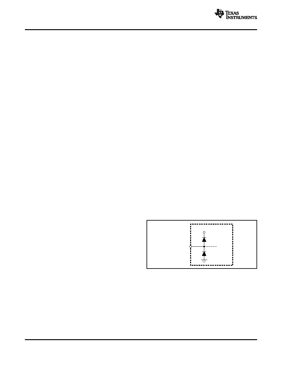
INPUT OVERVOLTAGE PROTECTION
OPERATING VOLTAGE
+V
S
External
Input/Output
Pin
Internal
Circuitry
SBOS468A – JUNE 2009 – REVISED JULY 2009.............................................................................................................................................................. www.ti.com
The THS7319 is targeted for triple-channel video
A 0.1-
F capacitor should be placed as close as
output
applications
that
require
three
possible to the power-supply pins to avoid potential
enhanced-definition (ED) video and/or RGB video
ringing or oscillation. Additionally, a large capacitor
output buffers. The THS7319 also supports standard
(such as 22
F to 100 F) should be placed on the
definition (SD) video for oversampled systems with
power-supply
line
to
minimize
interference
with
DAC sampling frequency of 54-MHz or greater.
50-/60-Hz line frequencies.
Although the THS7319 can be used for numerous
other applications, the needs and requirements of the
video
signal
are
the
most
important
design
The THS7319 input range allows for an input signal
parameters.
Built
on
the
revolutionary,
range from –0.06 V to approximately (VS+ – 1.5 V).
complementary Silicon Germanium (SiGe) BiCom3X
However, because of the internal fixed gain of 2 V/V
process, the THS7319 incorporates many features
(+6 dB) and the internal output level shift of 150 mV
not typically found in integrated video parts while
(typical), the output is generally the limiting factor for
consuming very low power. The THS7319 includes
the allowable linear input range. For example, with a
the following features:
5-V supply, the linear input range is from –0.06 V to
Single-supply 2.6-V to 5-V operation with low total
3.5 V. However, because of the gain and level shift,
quiescent current of 3.4 mA at 3.3 V and 3.7 mA
the linear output range limits the allowable linear
at 5 V
input range to approximately –0.06 V to 2.3 V.
Enable mode for shutting down the THS7319
amplifiers
to
save
system
power
in
power-sensitive applications
The THS7319 is built using a very high-speed,
DC input configuration with internal 150-mV dc
complementary, bipolar, and CMOS process. The
level
shifting
to
prevent
sync
crushing
and
internal junction breakdown voltages are relatively
saturation effects
low for these very small geometry devices. These
Third-order 20-MHz (–3-dB) low-pass filter for
breakdowns are reflected in the Absolute Maximum
DAC reconstruction or ADC image rejection ideal
Ratings table. All input and output device pins are
for:
protected with internal ESD protection diodes to the
–
NTSC/PAL
480p/576p
Y’P’BP’R or G’B’R’
power supplies, as shown in Figure 49.
(R’G’B’) signals
These diodes provide moderate protection to input
–
NTSC/PAL/SECAM composite video (CVBS),
overdrive voltages above and below the supplies as
S-Video Y’/C’, 480i/576i Y’P’BP’R, and G’B’R’
well. The protection diodes can typically support
(R’G’B’) signals for oversampled systems
30 mA of continuous current when overdriven.
Internally-fixed gain of 2-V/V (+6 dB) amplifiers
that
allows
for
dc-coupling
or
traditional
ac-coupling
Flow-through configuration using an ultra-small
MicrostarCSP package
The THS7319 is designed to operate from 2.6 V to
5 V over a –40°C to +85°C temperature range. The
impact on performance over the entire temperature
range is negligible as a result of the implementation
Figure 49. Internal ESD Protection
of thin film resistors and high-quality, low-temperature
coefficient capacitors. The design of the THS7319
allows
operation
down
to
2.5
V,
but
it
is
recommended to use at least a 2.7 V supply to
ensure that no issues arise with headroom or clipping
with 100% color-saturated CVBS signals. If only 75%
color saturated CVBS is supported, then the output
voltage requirements are reduced to 2 VPP on the
output, allowing a 2.6-V supply to be used without
issues.
16
Copyright 2009, Texas Instruments Incorporated
Product Folder Link(s): THS7319
相關(guān)PDF資料 |
PDF描述 |
|---|---|
| THS7360IPWR | VIDEO AMPLIFIER, PDSO20 |
| THS7360IPW | VIDEO AMPLIFIER, PDSO20 |
| THS7364IPWR | 6 CHANNEL, VIDEO AMPLIFIER, PDSO20 |
| THS7364IPW | 6 CHANNEL, VIDEO AMPLIFIER, PDSO20 |
| THS7365IPWR | 6 CHANNEL, VIDEO AMPLIFIER, PDSO20 |
相關(guān)代理商/技術(shù)參數(shù) |
參數(shù)描述 |
|---|---|
| THS7320 | 制造商:TI 制造商全稱:Texas Instruments 功能描述:3-Channel ED Filter Video Amplifier with 4-V/V Gain |
| THS7320IYHCR | 制造商:Texas Instruments 功能描述:3-CHANL ED FILTER VIDEO AMP, 4V/V GAIN - Tape and Reel 制造商:Texas Instruments 功能描述:IC 3-CH INTEG VIDEO AMP 9DSBGA 制造商:Texas Instruments 功能描述:Video Amplifiers 3-Ch ED Fltr Video Amp w/ 4V/V Gain 制造商:Texas Instruments 功能描述:3-Chanl ED Filter Video Amp, 4V/V Gain |
| THS7320IYHCT | 制造商:Texas Instruments 功能描述:IC 3-CH INTEG VIDEO AMP 9DSBGA |
| THS7320YHCEVM | 制造商:Texas Instruments 功能描述:THS7320YHCEVM - Boxed Product (Development Kits) 制造商:Texas Instruments 功能描述:Texas Instruments THS7320YHCEVM Development Kits 制造商:Texas Instruments 功能描述:MODULE EVAL FOR THS7320 ZSV 制造商:Texas Instruments 功能描述:EVAL BOARD, THS7320 VIDEO AMPLIFIER, Silicon Manufacturer:Texas Instruments, Silicon Core Number:THS7320, Kit Application Type:Amplifier, Application Sub Type:Video Buffer and Filter, Kit Contents:Eval Board THS7320 |
| THS7327 | 制造商:TI 制造商全稱:Texas Instruments 功能描述:3-Channel RGBHV Video Buffer with I2C Control, Selectable Filters, Monitor Pass-Thru,2:1 Input MUX, and Selectable Input Bias Modes |
發(fā)布緊急采購,3分鐘左右您將得到回復(fù)。