- 您現(xiàn)在的位置:買賣IC網(wǎng) > PDF目錄383946 > THS1206EVM (Texas Instruments, Inc.) THS1206 Evaluation Module(THS1206評(píng)估板) PDF資料下載
參數(shù)資料
| 型號(hào): | THS1206EVM |
| 廠商: | Texas Instruments, Inc. |
| 英文描述: | THS1206 Evaluation Module(THS1206評(píng)估板) |
| 中文描述: | THS1206評(píng)估模塊(THS1206評(píng)估板) |
| 文件頁(yè)數(shù): | 13/20頁(yè) |
| 文件大小: | 143K |
| 代理商: | THS1206EVM |
第1頁(yè)第2頁(yè)第3頁(yè)第4頁(yè)第5頁(yè)第6頁(yè)第7頁(yè)第8頁(yè)第9頁(yè)第10頁(yè)第11頁(yè)第12頁(yè)當(dāng)前第13頁(yè)第14頁(yè)第15頁(yè)第16頁(yè)第17頁(yè)第18頁(yè)第19頁(yè)第20頁(yè)
Digital Interface
2-3
Analog and Digital Interface
2.2
Digital Interface
The Modular THS1206EVM is designed for easy interfacing to multiple control
platforms. Jumper options are provided on the EVM to allow direct control over
the state of chip select pins (/CS0 and CS1) as well as the /RD pin.
Jumper W4 controls the signal applied to the active low CS0 pin. By completely
removing the shunt jumper located at W4, the CS0 pin is pulled low via a 10K
resistor R10. Used in combination with U2, an SN74AHC138 address
decoder, W4 allows the CS0 signal to be controlled by one of three different
addresses. Having the ability to select the address location of the ADC
provides the possibility of
stacking
additional parallel ADC or DAC boards with
the Modular THS1206EVM.
Jumpers W2 and W3 control signals applied to the RD and CS1 pins of the data
converter. Closing the jumpers allows the signals to be applied via the parallel
control connector J2. Opening the jumpers provides a logic high signal through
pull up resistors R6 and R7.
2.2.1
Parallel Control
Samtec part numbers SSW-110-22-F-D-VS-K and TSM-110-01-T-DV-P
provide a convenient ten-pin dual row header/socket combination at J2. This
header/socket provides access to the digital control pins of the EVM. Consult
Samtec at
www.samtec.com
or 1-800-SAMTEC-9 for a variety of mating
connector options.
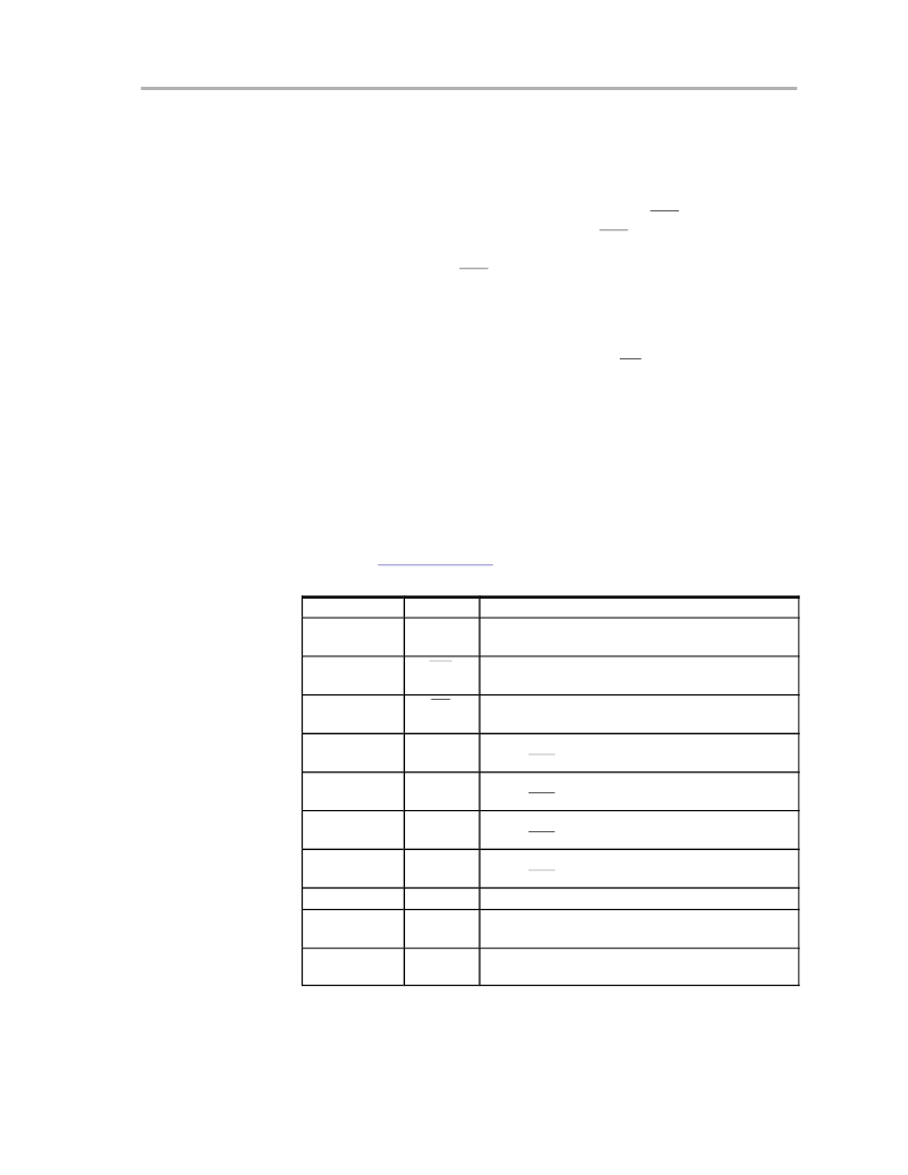
Pin Number
J2.1
Signal
DC_CSa
Description
Daughter card chip select
–
active low signal used to
access the EVM
J2.3
WR
DSP write strobe
–
active low signal used to initiate a
conversion
J2.5
RD
DSP read strobe
–
active low signal used to access
parallel data
J2.7
EVM_A0
EVM address line 0
–
used in conjunction with U2 to
control CS0
J2.9
EVM_A1
EVM address line 1
–
used in conjunction with U2 to
control CS0
EVM address line 2
–
used in conjunction with U2 to
control CS0
J2.11
EVM_A2
J2.13
EVM_A3
EVM address line 3
–
used in conjunction with U2 to
control CS0
J2.15
J2.17
EVM_A4
TOUT
EVM address line 4
–
not used
DSP timer input
–
optional CONVCLK or CONVST
source
J2.19
INT
DSP interrupt input
–
connects to the ADC DATA_AV
pin
相關(guān)PDF資料 |
PDF描述 |
|---|---|
| THS3001D | 420-MHz HIGH-SPEED CURRENT-FEEDBACK AMPLIFIERS |
| THS3002CDGN | 420-MHz HIGH-SPEED CURRENT-FEEDBACK AMPLIFIERS |
| THS3001DGN | 420-MHz HIGH-SPEED CURRENT-FEEDBACK AMPLIFIERS |
| THS3001EVM | 420-MHz HIGH-SPEED CURRENT-FEEDBACK AMPLIFIERS |
| THS3002 | 420-MHz HIGH-SPEED CURRENT-FEEDBACK AMPLIFIERS |
相關(guān)代理商/技術(shù)參數(shù) |
參數(shù)描述 |
|---|---|
| THS1206IDA | 功能描述:模數(shù)轉(zhuǎn)換器 - ADC 12-Bit 6 MSPS Quad Channel RoHS:否 制造商:Texas Instruments 通道數(shù)量:2 結(jié)構(gòu):Sigma-Delta 轉(zhuǎn)換速率:125 SPs to 8 KSPs 分辨率:24 bit 輸入類型:Differential 信噪比:107 dB 接口類型:SPI 工作電源電壓:1.7 V to 3.6 V, 2.7 V to 5.25 V 最大工作溫度:+ 85 C 安裝風(fēng)格:SMD/SMT 封裝 / 箱體:VQFN-32 |
| THS1206IDA | 制造商:Texas Instruments 功能描述:A/D CONVERTER ((NW)) |
| THS1206IDAG4 | 功能描述:模數(shù)轉(zhuǎn)換器 - ADC 12-Bit 6 MSPS Quad Channel RoHS:否 制造商:Texas Instruments 通道數(shù)量:2 結(jié)構(gòu):Sigma-Delta 轉(zhuǎn)換速率:125 SPs to 8 KSPs 分辨率:24 bit 輸入類型:Differential 信噪比:107 dB 接口類型:SPI 工作電源電壓:1.7 V to 3.6 V, 2.7 V to 5.25 V 最大工作溫度:+ 85 C 安裝風(fēng)格:SMD/SMT 封裝 / 箱體:VQFN-32 |
| THS1206IDAR | 功能描述:模數(shù)轉(zhuǎn)換器 - ADC 12-Bit 6 MSPS Quad Channel RoHS:否 制造商:Texas Instruments 通道數(shù)量:2 結(jié)構(gòu):Sigma-Delta 轉(zhuǎn)換速率:125 SPs to 8 KSPs 分辨率:24 bit 輸入類型:Differential 信噪比:107 dB 接口類型:SPI 工作電源電壓:1.7 V to 3.6 V, 2.7 V to 5.25 V 最大工作溫度:+ 85 C 安裝風(fēng)格:SMD/SMT 封裝 / 箱體:VQFN-32 |
| THS1206IDARG4 | 功能描述:模數(shù)轉(zhuǎn)換器 - ADC 12-Bit 6 MSPS Quad Channel RoHS:否 制造商:Texas Instruments 通道數(shù)量:2 結(jié)構(gòu):Sigma-Delta 轉(zhuǎn)換速率:125 SPs to 8 KSPs 分辨率:24 bit 輸入類型:Differential 信噪比:107 dB 接口類型:SPI 工作電源電壓:1.7 V to 3.6 V, 2.7 V to 5.25 V 最大工作溫度:+ 85 C 安裝風(fēng)格:SMD/SMT 封裝 / 箱體:VQFN-32 |
發(fā)布緊急采購(gòu),3分鐘左右您將得到回復(fù)。