- 您現在的位置:買賣IC網 > PDF目錄383990 > TDA9855WP (NXP SEMICONDUCTORS) I2C-bus controlled BTSC stereo/SAP decoder and audio processor PDF資料下載
參數資料
| 型號: | TDA9855WP |
| 廠商: | NXP SEMICONDUCTORS |
| 元件分類: | 消費家電 |
| 英文描述: | I2C-bus controlled BTSC stereo/SAP decoder and audio processor |
| 中文描述: | SPECIALTY CONSUMER CIRCUIT, PQCC68 |
| 文件頁數: | 9/52頁 |
| 文件大小: | 345K |
| 代理商: | TDA9855WP |
第1頁第2頁第3頁第4頁第5頁第6頁第7頁第8頁當前第9頁第10頁第11頁第12頁第13頁第14頁第15頁第16頁第17頁第18頁第19頁第20頁第21頁第22頁第23頁第24頁第25頁第26頁第27頁第28頁第29頁第30頁第31頁第32頁第33頁第34頁第35頁第36頁第37頁第38頁第39頁第40頁第41頁第42頁第43頁第44頁第45頁第46頁第47頁第48頁第49頁第50頁第51頁第52頁
1997 Nov 04
9
Philips Semiconductors
Product specification
I
2
C-bus controlled BTSC stereo/SAP
decoder and audio processor
TDA9855
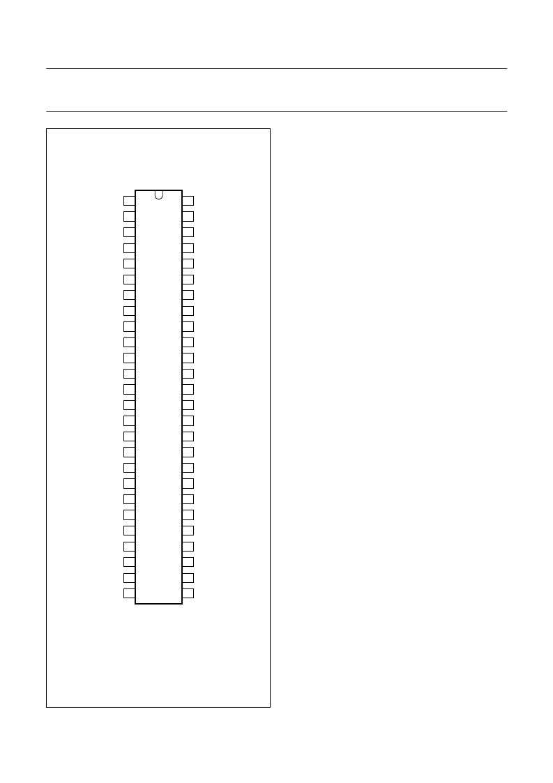
Fig.3 Pin configuration (SDIP version).
handbook, halfpage
TDA9855
MHA835
1
2
3
4
5
6
7
8
9
10
11
12
13
14
15
16
17
18
19
20
21
22
23
24
25
26
52
51
50
49
48
47
46
45
44
43
42
41
40
39
38
37
36
35
34
33
32
31
30
29
28
27
TL
TR
B1L
B1R
B2L
B2R
OUTS
SW
MAD
n.c.
OUTL
OUTR
LDL
LDR
VIL
VIR
EOL
EOR
CAV
CPS1
Vref
CPS2
LIL
LIR
AVL
AVR
SOL
SOR
LOL
LOR
CTW
CSS
CTS
CMO
CW
CER
Cs
CADJ
VEO
CPH
CP2
CNR
CP1
CM
VCAP
CDEC
COMP
GND
VCC
SDA
SCL
FUNCTIONAL DESCRIPTION
Decoder
I
NPUT LEVEL ADJUSTMENT
The composite input signal is fed to the input level
adjustment stage. In order to compensate tolerances of
the FM demodulator which supplied the composite input
signal, the TDA9855 provides an input level adjustment
stage. The control range is from
3.5 to +4.0 dB in steps of
0.5 dB. The subaddress control 3 of Tables 5 and 6 and
the level adjust setting of Table 22 allows an optimum
signal adjustment during the set alignment in the
production line. This value has to be stored in a
non-volatile memory. The maximum input signal voltage is
2 V (RMS).
S
TEREO DECODER
The output signal of the level adjustment stage is coupled
to a low-pass filter which suppresses the baseband noise
above 125 kHz. The composite signal is then fed into a
pilot detector/pilot cancellation circuit and into the MPX
demodulator. The main L + R signal passes a 75
μ
s fixed
de-emphasis filter and is fed into the dematrix circuit.
The decoded sub-signal L
R is sent to the stereo/SAP
switch. To generate the pilot signal the stereo demodulator
uses a PLL circuit including a ceramic resonator.
The stereo channel separation can be adjusted by an
automatic procedure or manually. For a detailed
description see Section “Adjustment procedure”.
The stereo identification can be read by the I
2
C-bus
(see Table 2). Two different pilot thresholds can be
selected via the I
2
C-bus (see Table 24).
SAP
DEMODULATOR
The composite signal is fed from the output of the input
level adjustment stage to the SAP demodulator circuit
through a 5f
H
(f
H
= horizontal frequency) band-pass filter.
The demodulator level is automatically controlled.
The SAP demodulator includes internal noise and field
strength detectors that mute the SAP output in the event of
insufficient signal conditions. The SAP identification signal
can be read by the I
2
C-bus (see Table 2).
S
WITCH
The stereo/SAP switch feeds either the L
R signal or the
SAP demodulator output signal via the internal dbx noise
reduction circuit to the dematrix/line out select circuit.
Table 21 shows the different switch modes provided at the
output pins LOR and LOL.
相關PDF資料 |
PDF描述 |
|---|---|
| TDA9859 | Universal hi-fi audio processor for TV |
| TDA9860 | Universal HiFi audio processor for TV |
| TDA9861 | Universal HiFi audio processor for TV |
| TDA9873 | Multistandard dual carrier stereo sound decoder |
| TDA9873H | Multistandard dual carrier stereo sound decoder |
相關代理商/技術參數 |
參數描述 |
|---|---|
| TDA9859 | 制造商:PHILIPS 制造商全稱:NXP Semiconductors 功能描述:Universal hi-fi audio processor for TV |
| TDA9859H | 制造商:PHILIPS 制造商全稱:NXP Semiconductors 功能描述:Universal hi-fi audio processor for TV |
| TDA9860 | 制造商:PHILIPS 制造商全稱:NXP Semiconductors 功能描述:Universal HiFi audio processor for TV |
| TDA9860/V2,112 | 功能描述:IC AUD PROCESSOR HIFI 32-SDIP RoHS:是 類別:集成電路 (IC) >> 線性 - 音頻處理 系列:- 其它有關文件:STA321 View All Specifications 標準包裝:1 系列:Sound Terminal™ 類型:音頻處理器 應用:數字音頻 安裝類型:表面貼裝 封裝/外殼:64-LQFP 裸露焊盤 供應商設備封裝:64-LQFP EP(10x10) 包裝:Digi-Reel® 其它名稱:497-11050-6 |
| TDA9860N | 制造商:PHILIPS 制造商全稱:NXP Semiconductors 功能描述:Universal HiFi audio processor for TV |
發(fā)布緊急采購,3分鐘左右您將得到回復。