- 您現(xiàn)在的位置:買賣IC網(wǎng) > PDF目錄383941 > TDA8443A (NXP SEMICONDUCTORS) I2C-bus controlled YUV/RGB switch PDF資料下載
參數(shù)資料
| 型號(hào): | TDA8443A |
| 廠商: | NXP SEMICONDUCTORS |
| 元件分類: | 運(yùn)動(dòng)控制電子 |
| 英文描述: | I2C-bus controlled YUV/RGB switch |
| 中文描述: | 6-CHANNEL, AUDIO/VIDEO SWITCH, PDIP24 |
| 封裝: | 0.600 INCH, PLASTIC, MO-015AD, SOT-101-1, DIP-24 |
| 文件頁(yè)數(shù): | 15/20頁(yè) |
| 文件大?。?/td> | 124K |
| 代理商: | TDA8443A |
第1頁(yè)第2頁(yè)第3頁(yè)第4頁(yè)第5頁(yè)第6頁(yè)第7頁(yè)第8頁(yè)第9頁(yè)第10頁(yè)第11頁(yè)第12頁(yè)第13頁(yè)第14頁(yè)當(dāng)前第15頁(yè)第16頁(yè)第17頁(yè)第18頁(yè)第19頁(yè)第20頁(yè)
1995 Mar 07
15
Philips Semiconductors
Product specification
I
2
C-bus controlled YUV/RGB switch
TDA8443A
Input clamps
The R, G, B respectively (R
Y), Y and (B
Y) video signals
are AC-coupled to the IC where they are clamped on the
black level. The timing information for this clamping action
is derived from the associated synchronization signal
SYNC, which could also consist of the composite video
information signal CVBS. The syncsignal is AC-coupled to
the IC where it is clamped on top-sync level, information
obtained from this action is used to generate the clamp
pulses.
The clamp pulses can be generated in two ways:
1.
Using the sync information (internal clamping)
The sync information is clamped on top-sync and the
information obtained from this action is used to switch
an internal current source at pin 24.
Pin 24 should be connected to V
P
via a 4.7 k
resistor,
and a 1 nF capacitor to ground. During video scan the
voltage at pin 24 will be HIGH (equals positive supply
voltage). During the synchronization pulses the
voltage at pin 24 will drop to zero because of the
current sink (2.5 mA).
When the synchronization pulse is over, the current
source is switched off and the voltage at pin 24 will rise
to its higher level. Because of the time constant at
pin 24, the restoration will take some microseconds.
The voltage at pin 24 is also sensed internally and at
the time it is between 0.456V
P
and 0.544V
P
, a time
pulse is generated and used for the clamping action.
Using a sandcastle pulse (external clamping)
If an associated sandcastle pulse is available, it can
also be used as a clamping pulse. In this event the
sandcastle pulse should be connected to pin 24, the
top of the clamping pulse should be between 0.544V
P
and 0.456V
P
. The timing of the internal clamping pulse
will be equal to the timing of the higher part of the
sandcastle pulse. If the sync signal is also connected,
the current sink will also become active during the
synchronization pulses. This means that the
sandcastle pulse should be connected to pin 24 via a
1 k
dropping resistor. In this event only the
sandcastle pulse at pin 24 will be influenced during
sync pulses, but the sandcastle pulse at the
sandcastle source will be unchanged.
2.
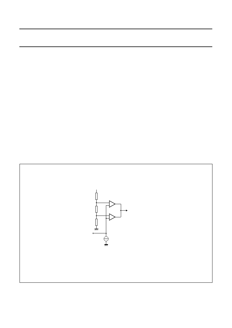
Fig.7 Clamping circuit.
Tolerance on V1 and V2 is given by
R/R and
V
P
/V
P
. The diffusion process gives
R/R (max) = 1.5%.
handbook, halfpage
MEA623
ON when current sync = 2.5 mA
OFF when current sync = 0 mA
pin 24
9.4 k
1.8 k
9.4 k
VP
V1
V2
clamp pulse
signal
V1 = 0.544 VP
V2 = 0.456 VP
相關(guān)PDF資料 |
PDF描述 |
|---|---|
| TDA8446 | Fast RGB/YC switch for digital decoding |
| TDA8446T | Fast RGB/YC switch for digital decoding |
| TDA8501 | PAL/NTSC encoder |
| TDA8501T | PAL/NTSC encoder |
| TDA8505 | SECAM encoder |
相關(guān)代理商/技術(shù)參數(shù) |
參數(shù)描述 |
|---|---|
| TDA8443AN | 制造商:未知廠家 制造商全稱:未知廠家 功能描述:TV Switch Circuit |
| TDA8444 | 制造商:PHILIPS 制造商全稱:NXP Semiconductors 功能描述:Octuple 6-bit DACs with I2C-bus |
| TDA8444AT | 制造商:PHILIPS 制造商全稱:NXP Semiconductors 功能描述:Octuple 6-bit DACs with I2C-bus |
| TDA8444AT/N4,112 | 功能描述:數(shù)模轉(zhuǎn)換器- DAC OCTUPLE 6-BIT D/A RoHS:否 制造商:Texas Instruments 轉(zhuǎn)換器數(shù)量:1 DAC 輸出端數(shù)量:1 轉(zhuǎn)換速率:2 MSPs 分辨率:16 bit 接口類型:QSPI, SPI, Serial (3-Wire, Microwire) 穩(wěn)定時(shí)間:1 us 最大工作溫度:+ 85 C 安裝風(fēng)格:SMD/SMT 封裝 / 箱體:SOIC-14 封裝:Tube |
| TDA8444AT/N4,115 | 功能描述:數(shù)模轉(zhuǎn)換器- DAC OCTUPLE 6-BIT D/A RoHS:否 制造商:Texas Instruments 轉(zhuǎn)換器數(shù)量:1 DAC 輸出端數(shù)量:1 轉(zhuǎn)換速率:2 MSPs 分辨率:16 bit 接口類型:QSPI, SPI, Serial (3-Wire, Microwire) 穩(wěn)定時(shí)間:1 us 最大工作溫度:+ 85 C 安裝風(fēng)格:SMD/SMT 封裝 / 箱體:SOIC-14 封裝:Tube |
發(fā)布緊急采購(gòu),3分鐘左右您將得到回復(fù)。