- 您現(xiàn)在的位置:買賣IC網(wǎng) > PDF目錄383989 > TDA8050A (NXP SEMICONDUCTORS) QPSK transmitter PDF資料下載
參數(shù)資料
| 型號: | TDA8050A |
| 廠商: | NXP SEMICONDUCTORS |
| 元件分類: | 通信及網(wǎng)絡(luò) |
| 英文描述: | QPSK transmitter |
| 中文描述: | SPECIALTY TELECOM CIRCUIT, PDSO32 |
| 封裝: | PLASTIC, SO-32 |
| 文件頁數(shù): | 5/28頁 |
| 文件大小: | 125K |
| 代理商: | TDA8050A |
第1頁第2頁第3頁第4頁當(dāng)前第5頁第6頁第7頁第8頁第9頁第10頁第11頁第12頁第13頁第14頁第15頁第16頁第17頁第18頁第19頁第20頁第21頁第22頁第23頁第24頁第25頁第26頁第27頁第28頁
1999 Nov 05
5
Philips Semiconductors
Product specification
QPSK transmitter
TDA8050A
FUNCTIONAL DESCRIPTION
The I and Q signals are balanced analog signals of
400 mV (p-p). These are mixed by two double balanced
mixers with the output signal generated by a first local
oscillator, to provide the modulated signal.
The modulated signal is then filtered by an IF filter. This
filtered signal, together a signal generated by a second
local oscillator, is converted by a balanced mixer to
produce the QPSK signal.
The QPSK signal is amplified by a gain controlled output
amplifier to a level suitable for transmission. The gain of
the amplifier is bus controlled and this amplifier can be
disabled when not transmitting, to provide signal
attenuation.
The amplified signal is applied to an on-chip amplifier with
two balanced outputs (open collector) connected to two
off-chip resistors (values 150
), in turn connected to 9 V.
The balanced outputs drive a 2 : 1 transformer (Siemens
V944) loaded with 75
, which gives an output level of
55 dBmV. The output frequency range of the transmitter is
5 to 65 MHz.
The frequency of the first local oscillator operates at twice
the frequency (i.e. 280 MHz), fixed by a PLL implemented
in the circuit.
Thefrequencyofthesecondlocaloscillatoroperatesinthe
145 to 205 MHz bandwidth and can be programmed
through the PLL implemented in the circuit.
The VCOs of both the first and second local oscillators
need an external LC tank circuit with two varicap diodes.
The data sent to the PLL is loaded in bursts framed by
signal EN. Programming rising clock edges and their
appropriate data bits are ignored until EN goes active
(LOW). The internal latches are updated with the latest
programming data when EN returns to inactive (HIGH).
Only the last 14 bits are stored in the programming
register.
No check is made on the number of clock pulses received
during the time that programming is enabled. If EN goes
high while CLK is still LOW, a wrong active clock edge will
be generated, causing a shift of the data bits. At power up,
EN should be HIGH. The lock detector output LOCK is
HIGH when both PLLs are in lock.
The main divider ratio and the reference divider ratios are
provided via the serial bus. A control register controls the
Digital-to-Analog-Converter (DAC), the output amplifier
and the charge pump currents (see Tables 1, 2 and 3).
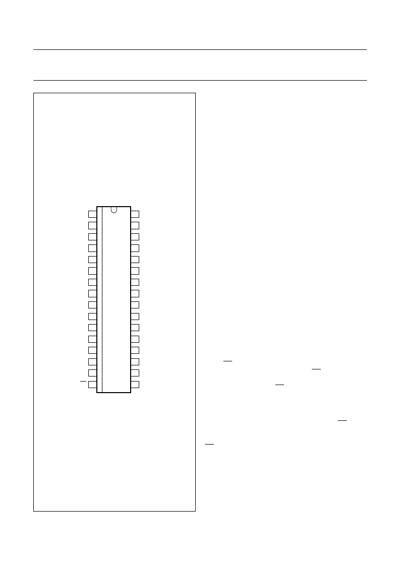
TDA8050A
FCE434
1
2
3
4
5
6
7
8
9
10
11
12
13
14
15
16
32
31
30
29
28
27
26
25
24
23
22
21
20
19
18
17
OUTEN
BUF_OUT
BUF_OUTC
AGND2
I_IN
I_INC
Q_IN
Q_INC
AGND1
TKAMOD
TKBMOD
CP_MOD
DVCC
CLK
SW_CAP
RF_INC
RF_IN
AVCC2
RF_OUTC
AVCC1
RF_OUT
IF_FILTC
IF_FILT
LOCK
TKACONV
TKBCONV
TUNECONV
CP_CONV
DATA
DGND
OSC_IN
EN
Fig.2 Pin configuration.
相關(guān)PDF資料 |
PDF描述 |
|---|---|
| TDA8315TD-G | TV/Video Sync Circuit |
| TDA837X | I2C-Bus Controlled Economy PAL/NTSC and NTSC TV-Processors |
| TDA8443AN | TV Switch Circuit |
| TDA8451 | |
| TDA8452 | |
相關(guān)代理商/技術(shù)參數(shù) |
參數(shù)描述 |
|---|---|
| TDA8050T | 制造商:PHILIPS 制造商全稱:NXP Semiconductors 功能描述:TDA8046H |
| TDA8051 | 制造商:PHILIPS 制造商全稱:NXP Semiconductors 功能描述:QPSK receiver |
| TDA8060ATS | 制造商:PHILIPS 制造商全稱:NXP Semiconductors 功能描述:Satellite ZERO-IF QPSK down-converter |
| TDA8060TS | 制造商:PHILIPS 制造商全稱:NXP Semiconductors 功能描述:Satellite ZERO-IF QPSK down-converter |
| TDA8083 | 制造商:PHILIPS 制造商全稱:NXP Semiconductors 功能描述:Satellite Demodulator and Decoder SDD3 |
發(fā)布緊急采購,3分鐘左右您將得到回復(fù)。