- 您現(xiàn)在的位置:買賣IC網(wǎng) > PDF目錄361412 > TC826CBU (Microchip Technology Inc.) Analog-to-Digital Converter with Bar Graph Display Output PDF資料下載
參數(shù)資料
| 型號: | TC826CBU |
| 廠商: | Microchip Technology Inc. |
| 元件分類: | 顯示驅(qū)動器 |
| 英文描述: | Analog-to-Digital Converter with Bar Graph Display Output |
| 中文描述: | 模擬與條形圖顯示數(shù)字轉(zhuǎn)換器輸出 |
| 文件頁數(shù): | 2/12頁 |
| 文件大小: | 122K |
| 代理商: | TC826CBU |
3-172
TELCOM SEMICONDUCTOR, INC.
ABSOLUTE MAXIMUM RATINGS*
Supply Voltage (V
+
to V
–
)............................................15V
Analog Input Voltage (either input)
(1)
................... V
+
to V
–
Power Dissipation (T
A
≤
70
°
C)
64-Pin Flat Package .........................................1.14W
Operating Temperature
‘C’ Devices.............................................0
°
C to +70
°
C
Storage Temperature ............................– 65
°
C to +150
°
C
Lead Temperature (Soldering, 10 sec) .................+300
°
C
*Static-sensitive device. Unused devices must be stored in conductive
material. Protect devices from static discharge and static fields. Stresses
above those listed under Absolute Maximum Ratings may cause perma-
nent damage to the device. These are stress ratings only and functional
operation of the device at these or any other conditions above those
indicated in the operational sections of the specifications is not implied.
Exposure to Absolute Maximum Rating Conditions for extended periods
may affect device reliability.
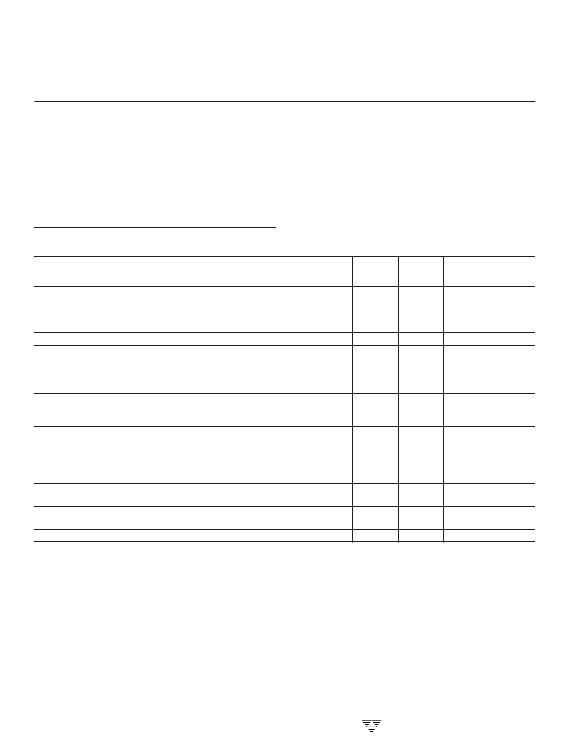
ELECTRICAL CHARACTERISTICS:
unless otherwise stated V
S
= 9V; R
OSC
= 430 k
; T
A
= 25
°
C; Full–Scale = 20 mV.
No. Symbol
Parameter
Test Conditions
Min
Typ
Max
Unit
1
2
—
—
Zero Input
Zero Reading Drift
V
IN
= 0.0V
V
IN
= 0.0V
0
°
C
≤
T
A
≤
+70
°
C
Max Deviation From
Best Straight Line
–V
IN
= +V
IN
V
IN
= 0V
V
IN
= 0V
VCM =
±
1V
V
IN
= 0V
0
≤
T
A
≤
+70
°
C
External Ref. Temperature
Coefficient = 0 ppm/
°
C
250k
Between
Common and V
+
0
°
C
≤
T
A
≤
+70
°
C
250k
Between
Common and V
DD
– 0
—
±
0
0.2
+0
1
Display
μ
V/
°
C
3
NL
Linearity Error
– 1
0.5
+1
Count
4
5
6
7
R/O
EN
ILK
CMRR
Rollover Error
Noise
Input Leakage Current
Common–Mode
Rejection Ratio
Scale Factor
Temperature Coefficient
– 1
—
—
—
0
+1
—
20
—
Count
μ
V
P–P
pA
μ
V/V
60
10
50
8
—
—
1
—
ppm/
°
C
9
VCTC
Analog Common
Temperature Coefficient
—
35
100
ppm/
°
C
10
V
COM
Analog Common
Voltage
LCD Segment
Drive Voltage
LCD Backplane
Drive Voltage
Power Supply Current
2.7
2.9
3.35
V
11
VSD
4
5
6
V
P–P
12
VBD
4
5
6
V
P–P
13
I
DD
—
125
175
μ
A
NOTES:
1. Input voltages may exceed the supply voltages when
the input current is limited to 100
μ
A.
2. Static sensitive device. Unused devices should be
stored in conductive material to protect devices from
static discharge and static fields.
3. Backplane drive is in phase with segment drive for ‘off’ segment and 180
°
C out of phase for ‘on’ segment. Frequency is 10 times
conversion rate.
4. Logic input pins 58, 59, and 60 should be connected through 1M
series resistors to V
SS
for logic 0.
TC826
A/D CONVERTER WITH
BAR GRAPH DISPLAY OUTPUT
相關(guān)PDF資料 |
PDF描述 |
|---|---|
| TC826CBU | A/D CONVERTER WITH BAR GRAPH DISPLAY OUTPUT |
| TC835CBU | PERSONAL COMPUTER DATA ACQUISITION A/D CONVERTER |
| TC835CBU | Personal Computer Data Acquisition A/D Converter |
| TC835CPI | Personal Computer Data Acquisition A/D Converter |
| TC835 | Personal Computer Data Acquisition A/D Converter |
相關(guān)代理商/技術(shù)參數(shù) |
參數(shù)描述 |
|---|---|
| TC826-TB | 制造商:Thomas & Betts 功能描述:CABLE TIE MOUNT, NYLON 6.6, NATURAL; Mount Fixing Type:Screw; Mount Material:Nylon 6.6; Mount Color:Natural; Accessory Type:Mounting Base; For Use With:Cable Ties ;RoHS Compliant: Yes 制造商:Thomas & Betts 功能描述:Cable Accessories Two Direction Mounting Base Bulk |
| TC-827-SC | 制造商:Thomas & Betts 功能描述: |
| TC828-0 | 制造商:Thomas & Betts 功能描述:CABLE TIE MT .4X.9 2-DIR 8SCREW BLK |
| TC828A | 制造商:TELCOM 制造商全稱:TelCom Semiconductor, Inc 功能描述:Switched Capacitor Voltage Converter |
| TC828AECT | 制造商:TELCOM 制造商全稱:TelCom Semiconductor, Inc 功能描述:Switched Capacitor Voltage Converter |
發(fā)布緊急采購,3分鐘左右您將得到回復(fù)。