- 您現(xiàn)在的位置:買賣IC網(wǎng) > PDF目錄98174 > TC7109CPL 1-CH 12-BIT DUAL-SLOPE ADC, PARALLEL ACCESS, PDIP40 PDF資料下載
參數(shù)資料
| 型號: | TC7109CPL |
| 元件分類: | ADC |
| 英文描述: | 1-CH 12-BIT DUAL-SLOPE ADC, PARALLEL ACCESS, PDIP40 |
| 封裝: | PLASTIC, DIP-40 |
| 文件頁數(shù): | 27/30頁 |
| 文件大?。?/td> | 479K |
| 代理商: | TC7109CPL |
第1頁第2頁第3頁第4頁第5頁第6頁第7頁第8頁第9頁第10頁第11頁第12頁第13頁第14頁第15頁第16頁第17頁第18頁第19頁第20頁第21頁第22頁第23頁第24頁第25頁第26頁當前第27頁第28頁第29頁第30頁
TC7109/A
DS21456C-page 6
2006 Microchip Technology Inc.
2.0
PIN DESCRIPTIONS
The descriptions of the pins are listed in Table 2-1.
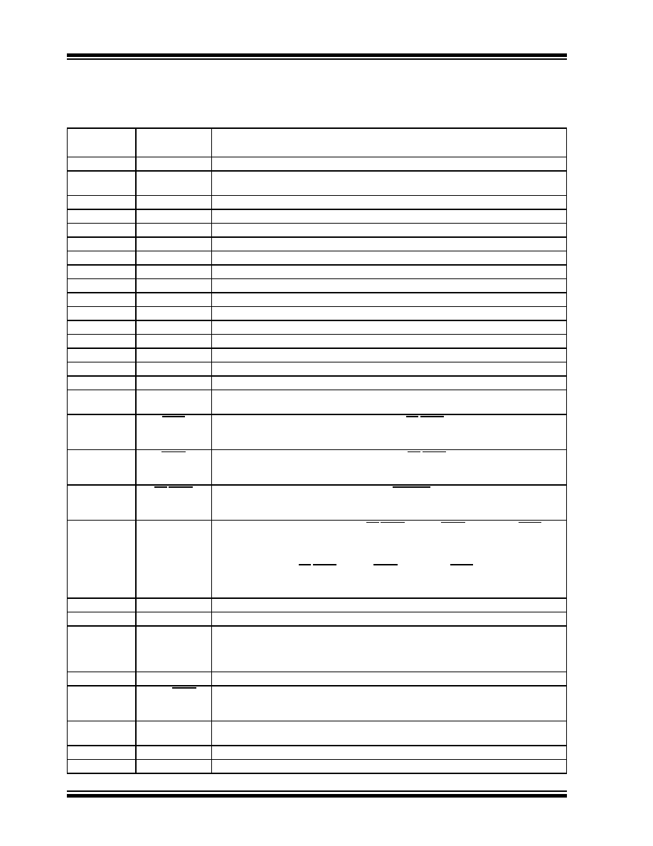
TABLE 2-1:
PIN FUNCTION TABLE
Pin Number
(40-Pin PDIP)
Symbol
Description
1
GND
Digital ground, 0V, ground return for all digital logic.
2
STATUS
Output HIGH during integrate and de-integrate until data is latched. Output LOW when
analog section is in auto-zero or zero integrator configuration.
3
POL
Polarity – High for positive input.
4
OR
Over Range – High if over ranged (Three-State Data bit).
5B12
Bit 12 (Most Significant bit) (Three-State Data bit).
6B11
Bit 11 (Three-State Data bit).
7B10
Bit 10 (Three-State Data bit).
8B9
Bit 9 (Three-State Data bit).
9B8
Bit 8 (Three-State Data bit).
10
B7
Bit 7 (Three-State Data bit).
11
B6
Bit 6 (Three-State Data bit).
12
B5
Bit 5 (Three-State Data bit).
13
B4
Bit 4 (Three-State Data bit).
14
B3
Bit 3 (Three-State Data bit).
15
B2
Bit 2 (Three-State Data bit).
B1
Bit 1 (Least Significant bit) (Three-State Data bit).
17
TEST
Input High – Normal operation. Input LOW – Forces all bit outputs HIGH.
Note: This input is used for test purposes only.
18
LBEN
Low Byte Enable – with MODE (Pin 21) LOW, and CE/LOAD (Pin 20) LOW, taking this pin
LOW activates low order byte outputs, B1–B8. With MODE (Pin 21) HIGH, this pin serves as
19
HBEN
High Byte Enable – with MODE (Pin 21) LOW, and CE/LOAD (Pin 20) LOW, taking this pin
LOW activates high order byte outputs, B9–B12, POL, OR. With MODE (Pin 21) HIGH, this
pin serves as high byte flag output used in Handshake mode. See Figures 3-7, 3-8, and 3-9.
20
CE/LOAD
Chip Enable/Load – with MODE (Pin 21) LOW, CE/LOAD serves as a master output enable.
When HIGH, B1–B12, POL, OR outputs are disabled. When MODE (Pin 21) is HIGH, a load
21
MODE
Input LOW – Direct Output mode where CE/LOAD (Pin 20), HBEN (Pin 19), and LBEN (Pin
18) act as inputs directly controlling byte outputs. Input Pulsed HIGH - Causes immediate
entry into Handshake mode and output of data as in Figure 3-9.
Input HIGH – enables CE/LOAD (Pin 20), HBEN (Pin 19), and LBEN (Pin 18) as outputs,
Handshake mode will be entered and data output as in Figure 3-7 and Figure 3-9
at conversions completion.
22
OSC IN
Oscillator Input.
23
OSC OUT
Oscillator Output.
24
OSC SEL
Oscillator Select – Input HIGH configures OSC IN, OSC OUT, BUFF OSC OUT as RC
oscillator – clock will be same phase and duty cycle as BUFF OSC OUT. Input LOW
configures OSC IN, OSC OUT for crystal oscillator - clock frequency will be 1/58 of frequency
at BUFF OSC OUT.
25
BUFF OSC OUT
Buffered Oscillator Output.
26
RUN/HOLD
Input HIGH – Conversions continuously performed every 8192 clock pulses.
Input LOW – Conversion in progress completed; converter will stop in auto-zero seven
counts before integrate.
27
SEND
Input - Used in Handshake mode to indicate ability of an external device to accept data.
Connect to V+ if not used.
28
V-
Analog Negative Supply – Nominally -5V with respect to GND (Pin 1).
29
REF OUT
Reference Voltage Output – Nominally 2.8V down from V+ (Pin 40).
相關(guān)PDF資料 |
PDF描述 |
|---|---|
| TC7109CLW713 | 1-CH 12-BIT DUAL-SLOPE ADC, PARALLEL ACCESS, PQCC44 |
| TC7109ACPL | 1-CH 12-BIT DUAL-SLOPE ADC, PARALLEL ACCESS, PDIP40 |
| TC7109CKW713 | 1-CH 12-BIT DUAL-SLOPE ADC, PARALLEL ACCESS, PQFP44 |
| TC7109ACKW | 12-BIT DUAL-SLOPE ADC, PARALLEL ACCESS, PQFP44 |
| TC7109ACPL | 12-BIT DUAL-SLOPE ADC, PARALLEL ACCESS, PDIP40 |
相關(guān)代理商/技術(shù)參數(shù) |
參數(shù)描述 |
|---|---|
| TC7109CPL | 制造商:Microchip Technology Inc 功能描述:IC 12BIT ADC 7109 DIP40 |
| TC7109CPL | 制造商:Microchip Technology Inc 功能描述:Special Function IC Package/Case:40-PDIP |
| TC7109IJL | 功能描述:模數(shù)轉(zhuǎn)換器 - ADC 13 Bit Fast Recovery RoHS:否 制造商:Texas Instruments 通道數(shù)量:2 結(jié)構(gòu):Sigma-Delta 轉(zhuǎn)換速率:125 SPs to 8 KSPs 分辨率:24 bit 輸入類型:Differential 信噪比:107 dB 接口類型:SPI 工作電源電壓:1.7 V to 3.6 V, 2.7 V to 5.25 V 最大工作溫度:+ 85 C 安裝風格:SMD/SMT 封裝 / 箱體:VQFN-32 |
| TC7-10-C100 | 功能描述:電纜固定件和配件 CBL STRAP W/ TACK NAIL RoHS:否 制造商:Heyco 類型:Cable Grips, Liquid Tight 材料:Nylon 顏色:Black 安裝方法:Cable 最大光束直徑:11.4 mm 抗拉強度: |
| TC7110A | 制造商:Thomas & Betts 功能描述:Fittings Connector 4inch Steel |
發(fā)布緊急采購,3分鐘左右您將得到回復(fù)。