- 您現(xiàn)在的位置:買賣IC網(wǎng) > PDF目錄361357 > T63H0006B-DX (TM Technology, Inc.) Li-Ion Battery Protector PDF資料下載
參數(shù)資料
| 型號: | T63H0006B-DX |
| 廠商: | TM Technology, Inc. |
| 英文描述: | Li-Ion Battery Protector |
| 中文描述: | 鋰離子電池保護器 |
| 文件頁數(shù): | 5/6頁 |
| 文件大小: | 52K |
| 代理商: | T63H0006B-DX |
TE
CH
tm
VD3/Excess Current Detector, Short Circuit
Protector
Both of the excess current detector and short
circuit protector can work when both control
FETs are in “ON” state. When the V- pin
voltage is going up to a value between the short
protection voltage Vshort/VDD and excess
current threshold VDET3, the excess current
detector operates and further soaring of V- pin
voltage higher than Vshort makes the short
circuit protector enabled. This leads the external
discharge control Nch MOSFET turn off with
the Dout pin being at “L” level.
An output delay time for the excess current
detector is internally fixed, 11ms typ. At
VDD=3.0V. Aquick recovery of V- pin level
from a value between Vshort and VDET3 within
the delay time keeps the discharge control FET
staying “H” state.
When the short circuit protector is enabled,
the Dout would be low and its delay time would
be 5us typ.
The V- pin has a built-in pulled down resistor,
typ. 130kOhm with connecting to the Vss pin.
After an excess current or short circuit
protection is detected, removing a cause of
excess current or external short circuit makes an
external discharge control FET to an “ON” state
automatically with the V- pin level being down
to the Vss level through pulled down resistor
built-in internally.
If VDD voltage would be higher than VDET2
at a time when the excess current is detected the
T63H0006B does not enter a standby mode, or
otherwise in case of lower VDD voltage than
VDET2 would lead the T63H0006B into a
standby.
After detecting short circuit the T63H0006B
will not enter a standby mode.
T63H0006B
TM Technology Inc. reserves the right
P. 5
Publication Date: JUN. 2004
to change products or specifications without notice. Revision:B
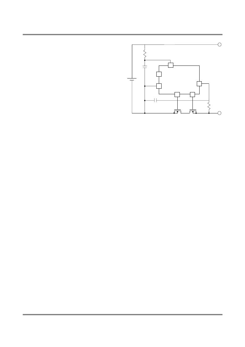
Application Circuits
6
5
4
3
2
1
-
C1
0.1uF
C2
0.1uF
R2
1 k ohm
T63H0006B
R1
100 ohm
+
Application Hints
R1 and C1 will stabilize a supply voltage to
the T63H0006B. A recommended R1 value is
less than 100 Ohm. A larger value of R1 leads
higher detection voltage, makes some errors,
because of shoot through current flowed in the
T63H0006B.
R2 and C2 will stabilize a V- pin voltage. The
resetting from over-discharge with connecting a
charger possibly be disabled by larger value of
R2.
Recommended value is less than 1kOhm.
After over-charge detection even connecting
battery pack to a system probably could not
allow a system to draw load current by a larger
R2xC2 time constant in the T63H0006B.
Recommended C2 value is less than 1uF.
R1 and R2 may cause power consumption over
rating of power dissipation of the T63H0006B
and a total of “R1+R2” should be more than
1kOhm.
The time constants R1xC1 or R2xC2 must
have a relation as below:
R1xC1<=R2xC2
Because in case that R1xC1, time constant for
VDD pin, would be larger than R2xC2, time
constant for V- pin then the T63H0006B might
be into a standby mode after detecting excess
current or short circuit current.
相關(guān)PDF資料 |
PDF描述 |
|---|---|
| T63H0006B | Li-Ion Battery Protector |
| T63H0008A | Li-Ion/Polymer Battery for one-cell Protector |
| T63H0008A-AX | Li-Ion/Polymer Battery for one-cell Protector |
| T63H0008A-BX | Li-Ion/Polymer Battery for one-cell Protector |
| T63H0008A-CX | Li-Ion/Polymer Battery for one-cell Protector |
相關(guān)代理商/技術(shù)參數(shù) |
參數(shù)描述 |
|---|---|
| T63H0008A | 制造商:TMT 制造商全稱:TMT 功能描述:Li-Ion/Polymer Battery for one-cell Protector |
| T63H0008A-AX | 制造商:TMT 制造商全稱:TMT 功能描述:Li-Ion/Polymer Battery for one-cell Protector |
| T63H0008A-BX | 制造商:TMT 制造商全稱:TMT 功能描述:Li-Ion/Polymer Battery for one-cell Protector |
| T63H0008A-CX | 制造商:TMT 制造商全稱:TMT 功能描述:Li-Ion/Polymer Battery for one-cell Protector |
| T63H0008A-DX | 制造商:TMT 制造商全稱:TMT 功能描述:Li-Ion/Polymer Battery for one-cell Protector |
發(fā)布緊急采購,3分鐘左右您將得到回復(fù)。