- 您現在的位置:買賣IC網 > PDF目錄361357 > T63H0001A-BX (TM Technology, Inc.) Li-Ion Battery Protector PDF資料下載
參數資料
| 型號: | T63H0001A-BX |
| 廠商: | TM Technology, Inc. |
| 英文描述: | Li-Ion Battery Protector |
| 中文描述: | 鋰離子電池保護器 |
| 文件頁數: | 3/7頁 |
| 文件大小: | 55K |
| 代理商: | T63H0001A-BX |
TE
CH
tm
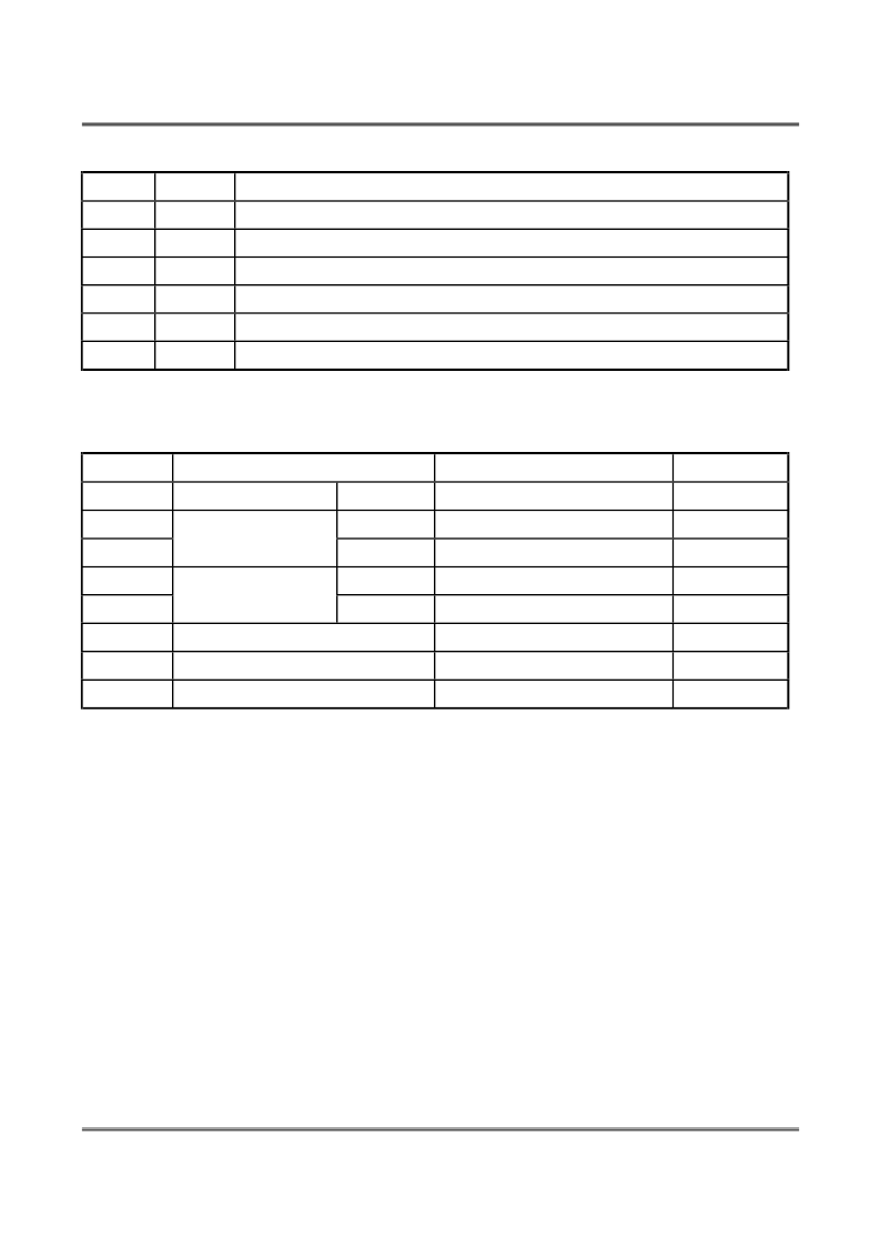
Pin description
Pin No.
1
2
3
4
5
6
ABSOLUTE MAXIMUM RATINGS
T63H0001A
TM Technology Inc. reserves the right
P. 3
to change products or specifications without notice.
Publication Date:MAR. 2004
Revision:A
Symbol Pin description
Cout
Output of over-charge detection, CMOS output
Ct
Pin for external capacitor setting output delay of VD1
Vss
Ground
Dout
Output of over-discharge detection, CMOS output
Vdd
Power supply
VM
Pin for charger negative input
Vss=0V
Symbol
Vdd
VM
Vct
Vcout
Vdout
Pd
Topt
Tstg
Absolute Maximum ratings are threshold limit values that must not be exceeded even for an instant
under any conditions. Moreover, such values for any two items must not be reached simultaneously.
Operation above these absolute maximum ratings may cause degradation or permanent damage to the
device. These are stress ratings only and do not necessarily imply functional operation below these
limits.
Item
Rating
-0.3 to 20
Vdd-20 to Vss+0.3
Vss-0.3 to Vss+0.3
Vdd-20 to Vss+0.3
Vss-0.3 to Vss+0.3
150
-40 to +85
-55 to +125
Unit
V
V
V
V
V
mV
oC
oC
Input Voltage
Vdd-VM
VM pin
Ct pin
Cout pin
Dout pin
Output Voltage
Power Dissipation
Operating Temperature Range
Storage Temperature Range
相關PDF資料 |
PDF描述 |
|---|---|
| T63H0001A-CX | Li-Ion Battery Protector |
| T63H0002A | T63H0002A |
| T63H0002A-AX | T63H0002A |
| T63H0002A-BX | T63H0002A |
| T63H0002A-CX | T63H0002A |
相關代理商/技術參數 |
參數描述 |
|---|---|
| T63H0001A-CX | 制造商:TMT 制造商全稱:TMT 功能描述:Li-Ion Battery Protector |
| T63H0002A | 制造商:TMT 制造商全稱:TMT 功能描述:T63H0002A |
| T63H0002A-AX | 制造商:TMT 制造商全稱:TMT 功能描述:T63H0002A |
| T63H0002A-BX | 制造商:TMT 制造商全稱:TMT 功能描述:T63H0002A |
| T63H0002A-CX | 制造商:TMT 制造商全稱:TMT 功能描述:T63H0002A |
發(fā)布緊急采購,3分鐘左右您將得到回復。