- 您現(xiàn)在的位置:買賣IC網(wǎng) > PDF目錄1970 > SY58627LMG (Micrel Inc)IC BUFF REC 6.4GBPS 32MLF PDF資料下載
參數(shù)資料
| 型號: | SY58627LMG |
| 廠商: | Micrel Inc |
| 文件頁數(shù): | 14/17頁 |
| 文件大?。?/td> | 0K |
| 描述: | IC BUFF REC 6.4GBPS 32MLF |
| 標(biāo)準(zhǔn)包裝: | 60 |
| 系列: | * |
Micrel, Inc.
SY58627L
January 2006
6
M9999-010606-A
hbwhelp@micrel.com or (408) 955-1690
Input Voltage (VIN)...................................................... -0.5V to VCC
Input Current (RXIN, /RXIN,
≤120mins) ............................... 67mA
CML Output Current (IOUT)
Continuous (
≤120mins)..................................................... 67mA
Surge .............................................................................. 100mA
Termination Current
VT.................................................................................. ±100mA
VREF-AC Current
Source/sink current on VREF-AC.......................................... ±2mA
Lead Temperature (soldering, 20 sec.) ..............................+260°C
Storage Temperature (TS) ..................................... -65°C to 150°C
Operating Ratings
(2)
Supply Voltage (VCC) .................................... +3.0V to +3.6V
Ambient Temperature (TA) ............................ -40°C to +85°C
Package Thermal Resistance
(3)
QFN (
θ
JA)
Still-Air ...............................................................34°C/W
QFN (
Ψ
JB)
Junction-to-Board ..............................................20°C/W
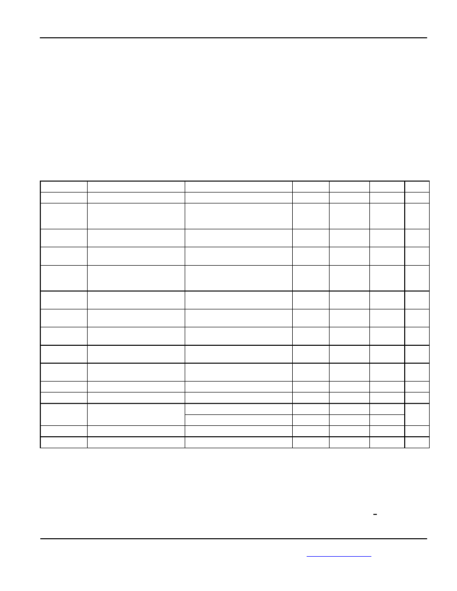
DC Electrical Characteristics
(4)
TA = -40°C to +85°C; unless otherwise stated.
Symbol
Parameter
Condition
Min
Typ
Max
Units
VCC
Power Supply
3.0
3.3
3.6
V
IEE
Power Supply Current
Max VCC, includes 50
internal
source resistors, no external load
current
210
260
mA
RIN
Input Resistance
(RXIN-to-VTTIN)
45
50
55
RDIFF_IN
Differential Input Resistance
(RXIN-to-/RXIN)
90
100
110
VIN_TRANS
Transmission Line Input
Voltage Swing
(RXIN, /RXIN)
Input signal swing applied to
transmission line input up to 36
in. (driver side of RXIN)
0.20
VPK
VIN
Input Voltage Swing
(RXIN, /RXIN)
See Figure 4a.
0.1
1.3
VPK
VDIFF_IN
Differential Input Voltage Swing
|RXIN-/RXIN|
See Figure 4b.
0.2
VPP
VIH
Input High Voltage
(RXIN, /RXIN)
VEE+1.6
VCC
V
VIL
Input LOW Voltage
(RXIN, /RXIN)
VEE+1.4
VIH-0.1
V
VTTIN
RXIN-to-VTTIN
(RXIN, /RXIN)
1.5
V
VTTIN Range
VTTIN Voltage Range
Voltage applied to VTTIN pin
VCC-1.5
VCC+1.5
V
VTTOUT Range
VTTOUT Voltage Range
Voltage applied to VTTOUT pin
VCC-0.4
VCC
V
LOS
Loss-of-Signal Input Levels
Signal-detect Assert
110
mVPK
Signal-detect De-assert
90
Input Return Loss
100MHz to 3.5GHz
10
dB
VREF-AC
Output Reference Voltage
VCC-0.95
VCC-0.84
VCC-0.7
V
Notes:
1.
Permanent device damage may occur if absolute maximum ratings are exceeded. This is a stress rating only and functional operation is
not implied at conditions other than those detailed in the operational sections of this data sheet. Exposure to absolute maximum ratings
conditions for extended periods may affect device reliability.
2.
The data sheet limits are not guaranteed if the device is operated beyond the operating ratings.
3.
Package thermal resistance assumes exposed pad is soldered (or equivalent) to the devices most negative potential on the PCB.
θ
JA and
Ψ
JB values are determined for a 4-layer board in still air unless otherwise stated.
4.
The circuit is designed to meet the DC specifications shown in the above table after thermal equilibrium has been established. TJ < 125°C.
相關(guān)PDF資料 |
PDF描述 |
|---|---|
| SY87724LHY | IC MUX/DEMUX 3X1 80LQFP |
| SY89540UMG TR | IC XPOINT SWITCH 4X4 LVDS 44-MLF |
| T89C5115-TISUM | IC 8051 MCU FLASH 16K 28SOIC |
| T89C51AC2-SLSIM | IC 8051 MCU FLASH 32K 44PLCC |
| T89C51CC01UA-7CTIM | IC 8051 MCU FLASH 32K 64BGA |
相關(guān)代理商/技術(shù)參數(shù) |
參數(shù)描述 |
|---|---|
| SY58627LMG TR | 功能描述:緩沖器和線路驅(qū)動器 6.4Gbps Receiver w/ Equalization (I Temp, Green) RoHS:否 制造商:Micrel 輸入線路數(shù)量:1 輸出線路數(shù)量:2 極性:Non-Inverting 電源電壓-最大:+/- 5.5 V 電源電壓-最小:+/- 2.37 V 最大工作溫度:+ 85 C 安裝風(fēng)格:SMD/SMT 封裝 / 箱體:MSOP-8 封裝:Reel |
| SY58627LMGTR | 制造商:MICREL 制造商全稱:Micrel Semiconductor 功能描述:DC-to-6.4Gbps Backplane Receive Buffer with Four Stage Programmable Equalization and DC-Offset Control |
| SY58627LMG-TR | 功能描述:RECEIVER 6.4GBPS W/EQUALIZATION 制造商:microchip technology 系列:* 零件狀態(tài):過期 標(biāo)準(zhǔn)包裝:1 |
| SY5A00-5U1 | 制造商:SMC 功能描述:SY5000 5 port solenoid valve 2 x 3/2 24V |
| SY5B00-5U1 | 制造商:SMC 功能描述:SY5000 5 port solenoid valve 2 x 3/2 24V |
發(fā)布緊急采購,3分鐘左右您將得到回復(fù)。