- 您現(xiàn)在的位置:買賣IC網(wǎng) > PDF目錄98143 > ST52F513Y1B6 (STMICROELECTRONICS) 8-BIT, FLASH, 24 MHz, MICROCONTROLLER, PDIP16 PDF資料下載
參數(shù)資料
| 型號(hào): | ST52F513Y1B6 |
| 廠商: | STMICROELECTRONICS |
| 元件分類: | 微控制器/微處理器 |
| 英文描述: | 8-BIT, FLASH, 24 MHz, MICROCONTROLLER, PDIP16 |
| 封裝: | PLASTIC, DIP-16 |
| 文件頁(yè)數(shù): | 86/106頁(yè) |
| 文件大小: | 648K |
| 代理商: | ST52F513Y1B6 |
第1頁(yè)第2頁(yè)第3頁(yè)第4頁(yè)第5頁(yè)第6頁(yè)第7頁(yè)第8頁(yè)第9頁(yè)第10頁(yè)第11頁(yè)第12頁(yè)第13頁(yè)第14頁(yè)第15頁(yè)第16頁(yè)第17頁(yè)第18頁(yè)第19頁(yè)第20頁(yè)第21頁(yè)第22頁(yè)第23頁(yè)第24頁(yè)第25頁(yè)第26頁(yè)第27頁(yè)第28頁(yè)第29頁(yè)第30頁(yè)第31頁(yè)第32頁(yè)第33頁(yè)第34頁(yè)第35頁(yè)第36頁(yè)第37頁(yè)第38頁(yè)第39頁(yè)第40頁(yè)第41頁(yè)第42頁(yè)第43頁(yè)第44頁(yè)第45頁(yè)第46頁(yè)第47頁(yè)第48頁(yè)第49頁(yè)第50頁(yè)第51頁(yè)第52頁(yè)第53頁(yè)第54頁(yè)第55頁(yè)第56頁(yè)第57頁(yè)第58頁(yè)第59頁(yè)第60頁(yè)第61頁(yè)第62頁(yè)第63頁(yè)第64頁(yè)第65頁(yè)第66頁(yè)第67頁(yè)第68頁(yè)第69頁(yè)第70頁(yè)第71頁(yè)第72頁(yè)第73頁(yè)第74頁(yè)第75頁(yè)第76頁(yè)第77頁(yè)第78頁(yè)第79頁(yè)第80頁(yè)第81頁(yè)第82頁(yè)第83頁(yè)第84頁(yè)第85頁(yè)當(dāng)前第86頁(yè)第87頁(yè)第88頁(yè)第89頁(yè)第90頁(yè)第91頁(yè)第92頁(yè)第93頁(yè)第94頁(yè)第95頁(yè)第96頁(yè)第97頁(yè)第98頁(yè)第99頁(yè)第100頁(yè)第101頁(yè)第102頁(yè)第103頁(yè)第104頁(yè)第105頁(yè)第106頁(yè)

ST52F510/F513/F514
80/106
Recognition of a STOP condition transfers data
received
from
the
Recovery
Buffer
to
the
SCDR_RX buffer, adding the eventual ninth data
bit. After this operation, RXF flag (bit 5) of SCI
Status Input Register is set to logic level 1. The
Control Unit reads data from the SCDR_RX buffer
(in read-only mode) by reading the SCI_IN Input
Register (address
36 024h) with the LDRI
instruction and provides a reset at logic level 0 to
the RXF flag.
If data of the Recovery Buffer is ready to be
transferred into the SCDR_RX buffer, but the
previous one has not been read by the Core, an
OVERRUN Error takes place: the SCI Status
Register flag OVERR (bit 4) indicates the error
condition. In this case, information that is stored in
the SCDR_RX buffer is not altered, but the one
that has caused the OVERRUN error can be
overwritten by new data deriving from the serial
data line.
13.1.1 Recovery Buffer Block .
This block is structured as a synchronized finite
state machine on the CLOCK_RX signal.
When the Recovery Buffer Block is in IDLE state it
waits for the reception of the correct 1 and 0
sequence representing START.
Recognition takes place by sampling the input RX
at CLOCK_RX frequency, which has a frequency
that is 16 times higher than CLOCK_TX. For this
reason, while the external transmitter sends a
single bit, the Recovery Buffer Block samples 16
states (from SAMPLE1 to SAMPLE16).
Analysis of the RX input signal is carried out by
checking three samples for each bit received.
If these three samples are not equal, then the
noise error flag, NSERR (bit 7), of SCI Status
Register is set to 1 and the data received value will
be the one assumed by the majority of the
samples.
The procedure described above, allows SCI not to
becomes IDLE, because of a limited noise due to
an erroneous sampling, the transmission is
recognized as correct and the noise flag error is
set.
At the end of the cycle of the reception of a bit, the
Recovery Buffer Block will repeat the same steps 9
times: one step for each bit received, plus one for
the stop acquisition (10 times in case of 9-bit data,
double stop or parity check).
At the end of data reception the Recovery Buffer
Block will supply information about eventual frame
errors by setting the 1 FRERR flag (bit 6) of the SCI
Status Register to 1.
A frame error can occur if the parity check hasn’t
been successfully achieved or if the STOP bit has
not been detected.
If
the
Recovery
Buffer
Block
receives
10
consecutive bits at logic level 0, a Line Break
condition occurs and the related Interrupt Request
is sent.
13.1.2 SCDR_RX Block.
It is a finite state machine synchronized with the
clock master signal, CKM.
The SCDR_RX block waits for the signal of
complete reception from the Recovery Buffer in
order to load the word received. Moreover, the
SCDR_RX block loads the values of FRERR and
NSERR flag bits of the Status Register, and sets
the RXF flag to 1.
By using the LDRI instruction data is transferred to
Register File and RXF flag is reset to 0, to indicate
that the SCDR_RX block is empty.
If new data arrives before the previous one has
been transferred to Register File, the overrun error
occurs and the OVERR flag of Status Register is
set to 1.
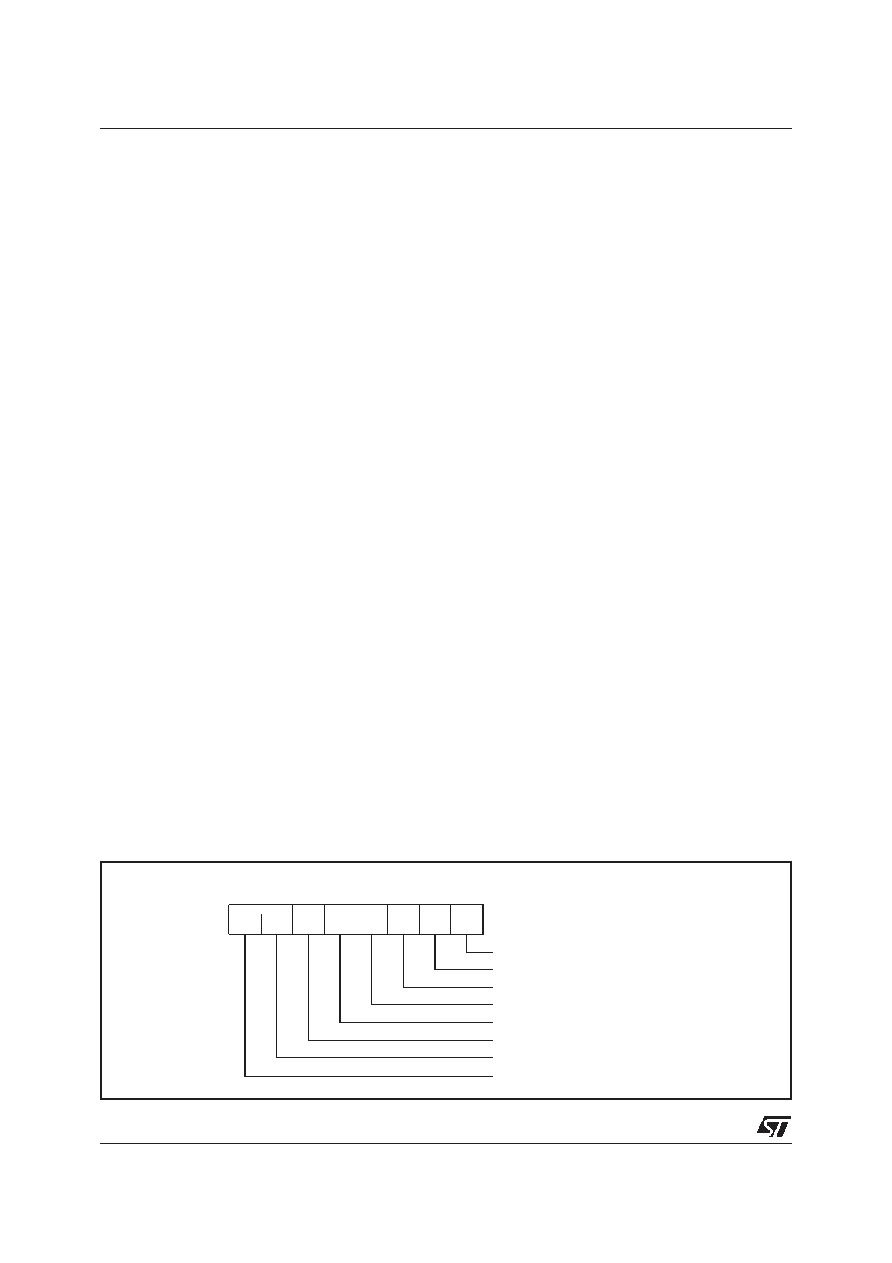
Figure 13.3 SCI Status Register
D7 D6 D5 D4 D3 D2 D1 D0
SCI STATUS REGISTER
TXEND
- END TRANSMISSION
TXEM
- TRANSMISSION DATA REGISTER EMPTY
R8
- RECEIVED NINTH BIT
NSERR
- NOISE ERROR
NOT USED
OVERR
- OVERRUN ERROR
RXF
- RECEIVE DATA REGISTER FULL
FRERR
- FRAME ERROR
相關(guān)PDF資料 |
PDF描述 |
|---|---|
| ST52F513Y2B6 | 8-BIT, FLASH, 24 MHz, MICROCONTROLLER, PDIP16 |
| ST52F510Y3B6 | 8-BIT, FLASH, 24 MHz, MICROCONTROLLER, PDIP16 |
| ST52F514Y2B6 | 8-BIT, FLASH, 24 MHz, MICROCONTROLLER, PDIP16 |
| ST52T430K3B6 | 8-BIT, OTPROM, 20 MHz, MICROCONTROLLER, PDIP32 |
| ST52T430K3T6 | 8-BIT, OTPROM, 20 MHz, MICROCONTROLLER, PQFP32 |
相關(guān)代理商/技術(shù)參數(shù) |
參數(shù)描述 |
|---|---|
| ST52F513Y3M6 | 制造商:STMicroelectronics 功能描述: |
| ST52F513YMM6 | 制造商:STMICROELECTRONICS 制造商全稱:STMicroelectronics 功能描述:8-BIT INTELLIGENT CONTROLLER UNIT ICU Two Timer/PWMs, ADC, I2C, SPI, SCI |
| ST52F514 | 制造商:STMICROELECTRONICS 制造商全稱:STMicroelectronics 功能描述:8-BIT INTELLIGENT CONTROLLER UNIT ICU Two Timer/PWMs, ADC, I2C, SPI, SCI |
| ST52F514F0B6 | 制造商:未知廠家 制造商全稱:未知廠家 功能描述:Microcontroller |
| ST52F514F0M6 | 制造商:未知廠家 制造商全稱:未知廠家 功能描述:Microcontroller |
發(fā)布緊急采購(gòu),3分鐘左右您將得到回復(fù)。