- 您現(xiàn)在的位置:買賣IC網(wǎng) > PDF目錄299919 > SP98608BDG (ZARLINK SEMICONDUCTOR INC) PARALLEL, 8 BITS INPUT LOADING, 0.002 us SETTLING TIME, 8-BIT DAC, CDIP24 PDF資料下載
參數(shù)資料
| 型號: | SP98608BDG |
| 廠商: | ZARLINK SEMICONDUCTOR INC |
| 元件分類: | DAC |
| 英文描述: | PARALLEL, 8 BITS INPUT LOADING, 0.002 us SETTLING TIME, 8-BIT DAC, CDIP24 |
| 封裝: | CERAMIC, DIP-24 |
| 文件頁數(shù): | 5/7頁 |
| 文件大小: | 312K |
| 代理商: | SP98608BDG |
SP98608
4
FT (Feedthrough)
The FT input allows both transparent or latched data
inputs. When open circuits this pin will self bias to -2V and
the data will be retained by the input latch for one half clock
cycle.
When the FT input is connected to 0V the input latch will
be transparent. In this mode, it is essential that the input
data has low time skew (<100ps) to avoid output glitches.
Multiplying Mode
Multiplying operation of the DAC is available in two
modes: either a voltage applied in place of the internal
reference, or a current supplied via the current set pin.
Voltage
Multiplying.
The
transfer
function
is
approximately: IOUT (Full Scale) = 4 x VIN/RSET. While this
mode offers the best linearity of operation, the frequency
response limitations mean that the maximum usable
bandwidth is limited to approximately 50MHz.
Current Multiplying. A circuit for using the DAC in
current multiplying mode is shown in Fig. 4. The transfer
function is approximately; IOUT (Full Scale) = 4 x IIN. In this
mode the current setting loop amplier is not used.
The operational bandwidth of the current input to -3dB is
at least 320MHz.
A 1V output is obtained into 25 ohm when a current of
approximately 11mA is fed into pin 1 and the input code is
selected for full output current.
Output Compliance
Using the SP98608 with a load resistor not referred to
ground, allows a larger output swing than the conventional
connection of Fig. 3. Connecting analog ground and the
current-setting resistor RSET to the load return supply
ensures that the scale factor of the output is independent of
the load.
Extending the compliance beyond +1V may cause slight
degradation of linearity; +3V should be considered an
absolute maximum.
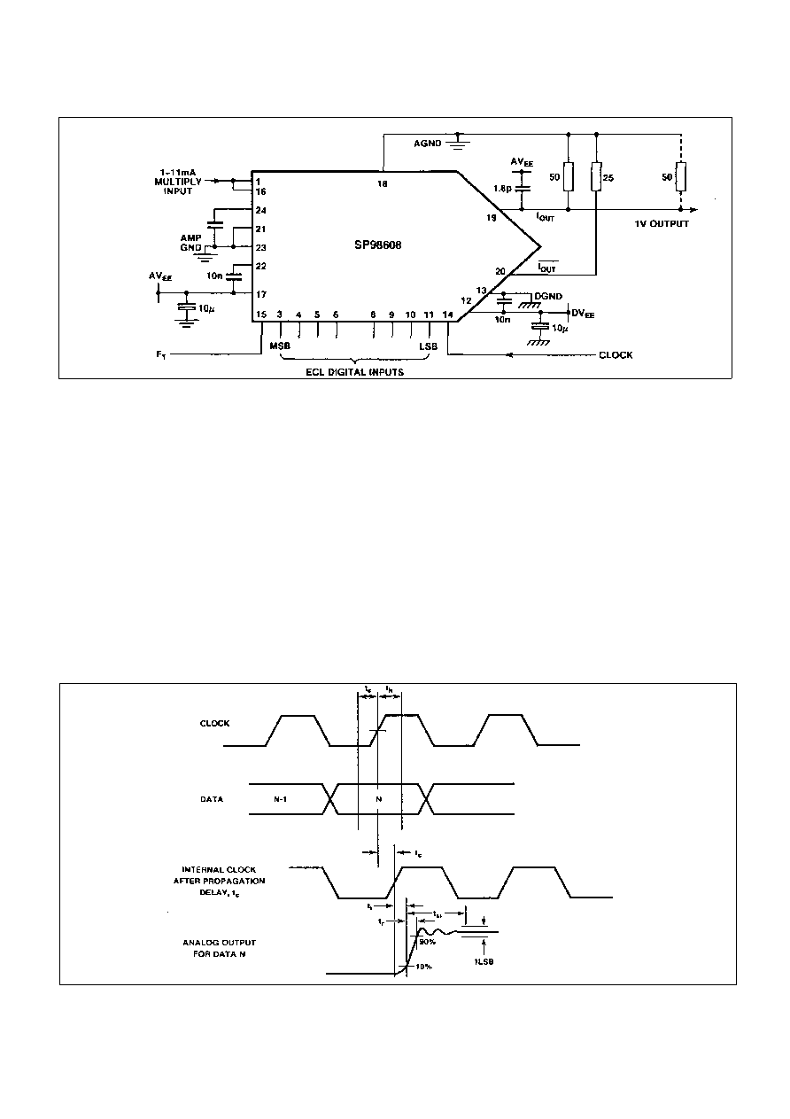
Fig.4 Current multiplying mode
Fig.5 Timing diagram - latched mode
相關(guān)PDF資料 |
PDF描述 |
|---|---|
| SPAKD56366PV120 | 24-BIT, 120 MHz, OTHER DSP, PQFP144 |
| SPB3 | RECTANGULAR CONNECTOR |
| SPB4 | RECTANGULAR CONNECTOR |
| SPB5 | RECTANGULAR CONNECTOR |
| SPBH5 | RECTANGULAR CONNECTOR |
相關(guān)代理商/技術(shù)參數(shù) |
參數(shù)描述 |
|---|---|
| SP9908 | 制造商:BOTHHAND 制造商全稱:Bothhand USA, LP. 功能描述:39 Watts Switching Power Supply |
| SP9909 | 制造商:BOTHHAND 制造商全稱:Bothhand USA, LP. 功能描述:40~62 Watts Switching Power Supply |
| SP9909A | 制造商:BOTHHAND 制造商全稱:Bothhand USA, LP. 功能描述:40~62 Watts Switching Power Supply |
| SP9919 | 制造商:BOTHHAND 制造商全稱:Bothhand USA, LP. 功能描述:25 Watts Switching Power Supply |
| SP9919A | 制造商:BOTHHAND 制造商全稱:Bothhand USA, LP. 功能描述:25 Watts Switching Power Supply |
發(fā)布緊急采購,3分鐘左右您將得到回復(fù)。