- 您現(xiàn)在的位置:買賣IC網(wǎng) > PDF目錄1969 > SP505BCM-L (Exar Corporation)IC TXRX WAN MULTI-MODE 80LQFP PDF資料下載
參數(shù)資料
| 型號: | SP505BCM-L |
| 廠商: | Exar Corporation |
| 文件頁數(shù): | 10/35頁 |
| 文件大?。?/td> | 0K |
| 描述: | IC TXRX WAN MULTI-MODE 80LQFP |
| 標準包裝: | 84 |
| 類型: | 收發(fā)器 |
| 驅(qū)動器/接收器數(shù): | 7/7 |
| 規(guī)程: | 多協(xié)議 |
| 電源電壓: | 5V |
| 安裝類型: | 表面貼裝 |
| 封裝/外殼: | 80-LQFP |
| 供應商設備封裝: | 80-LQFP(14x14) |
| 包裝: | 托盤 |
第1頁第2頁第3頁第4頁第5頁第6頁第7頁第8頁第9頁當前第10頁第11頁第12頁第13頁第14頁第15頁第16頁第17頁第18頁第19頁第20頁第21頁第22頁第23頁第24頁第25頁第26頁第27頁第28頁第29頁第30頁第31頁第32頁第33頁第34頁第35頁
8
Exar Coporation 48720 Kato Road, Fremont CA, 94538 (50) 668-7000 Fax (50) 668-707 www.exar.com
SP505_00_08308
+4V to +6V during an open-circuit (no
load). The charge pump would need to
be regulated down from +0V to +5V.
A typical +0V charge pump would require
external clamping such as 5V zener diodes
on V
DD and VSS to ground. The +5V output
hassymmetricallevelsasinthe+0Voutput.
The+5Visusedinthefollowingmodeswhere
RS-423 (V.0) are used: RS-449, EIA-530,
EIA-530A and V.36.
Phase 1 (±10V)
—V
SS charge storage — During this phase of
theclockcycle,thepositivesideofcapacitors
C
and C2 are initially charged to +5V. Cl
+
is
then switched to ground and the charge on
C
–
is transferred to C
2
–
. Since C
2
+
is con-
nected to +5V, the voltage potential across
capacitor C
2 is now 0V.
Phase 1 (±5V)
— V
SS & VDD charge storage and transfer
— With the C
and C2 capacitors initially
chargedto+5V,C
l
+
isthenswitchedtoground
andthechargeonC
–
istransferredtotheV
SS
storage capacitor. Simultaneously the C
2
–
is
switched to ground and 5V charge on C
2
+
is
transferred to the V
DD storage capacitor.
FEATURES…
The SP505 is a highly integrated serial
transceiver that allows software control of
its interface modes. Similar to the SP504,
the SP505 offers the same hardware inter-
face modes for RS-232 (V.28), RS-422A
(V.), RS-449, RS-485, V.35, EIA-530 and
includes V.36 and EIA-530A. The interface
mode selection is done via a 4–bit switch
for the drivers and receivers. The SP505
is fabricated using low–power BiCMOS
process technology, and incorporates a
Exar–patented (5,306,954) charge pump
allowing +5V only operation. Each device
is packaged in an 80–pin JEDEC Quad
FlatPack package.
The SP505 is ideally suited for wide area
network connectivity based on the interface
modes offered and the driver and receiver
configurations. The SP505 has seven (7)
independent drivers and seven (7) indepen-
dent receivers. In V.35 mode, the SP505
includes the necessary components and
termination resistors internal within the de-
vice for compliant V.35 operation.
THEORY OF OPERATION
The SP505 is made up of five separate
circuit blocks — the charge pump, drivers,
receivers,decoderandswitchingarray. Each
of these circuit blocks is described in more
detail below.
Charge–Pump
The SP505 charge pump is based on the
SP504designwhereExar'spatentedcharge
pump design (5,306,954) uses a four–phase
voltageshiftingtechniquetoattainsymmetri-
cal 0V power supplies. The charge pump
still requires external capacitors to store the
charge. In addition the SP504 charge pump
supplies +0V or +5V on V
SS and VDD de-
pending on the mode of operation. There is
afree–runningoscillatorthatcontrolsthefour
phases of the voltage shifting. A description
of each phase follows.
The SP505 charge pump is used for RS-
232 where the output voltage swing is
typically +0V and also used for RS-423.
However, RS-423 requires the voltage
swing on the driver output be between
V CC = +5V
–5V
+5V
V DD S torage C apa citor
C 1
C 2
C 4
+
–
VSS Storage C apa citor
C 3
+
–
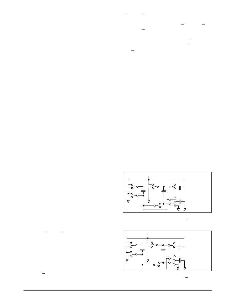
Figure 46. Charge Pump Phase for +5V.
V CC = +5V
V DD S torage C apa citor
C 1
C 2
C 4
+
–
VSS Storage C apa citor
C 3
+
–
–5V
Figure 45. Charge Pump Phase for +0V.
相關(guān)PDF資料 |
PDF描述 |
|---|---|
| SP506CM-L | IC TXRX WAN MULTI-MODE 80LQFP |
| SP507CM-L | IC TXRX WAN MULTI-MODE 80LQFP |
| SP508EF-L | IC TXRX MULTIPROTOCOL 100LQFP |
| SP510CM-L | IC TXRX MULTIPROTOCOL HS 100LQFP |
| SP526CF-L | IC TXRX WAN MULTI-MODE 44LQFP |
相關(guān)代理商/技術(shù)參數(shù) |
參數(shù)描述 |
|---|---|
| SP505CF | 制造商:SIPEX 制造商全稱:Sipex Corporation 功能描述:Multi-Protocol Serial Transceivers |
| SP505EB | 制造商:SIPEX 制造商全稱:Sipex Corporation 功能描述:Multi-Protocol Serial Transceivers |
| SP505EK | 制造商:SIPEX 制造商全稱:Sipex Corporation 功能描述:Multi-Protocol Serial Transceivers |
| SP505P | 制造商:SII 制造商全稱:Seiko Instruments Inc 功能描述:LIQUID CRYSTAL DISPLAYS(STANDARD PRODUCTS) |
| SP505RB | 制造商:SIPEX 制造商全稱:Sipex Corporation 功能描述:Multi-Protocol Serial Transceivers |
發(fā)布緊急采購,3分鐘左右您將得到回復。