- 您現(xiàn)在的位置:買賣IC網(wǎng) > PDF目錄1969 > SP504MCM-L (Exar Corporation)IC TXRX WAN MULTI-MODE 80LQFP PDF資料下載
參數(shù)資料
| 型號: | SP504MCM-L |
| 廠商: | Exar Corporation |
| 文件頁數(shù): | 12/32頁 |
| 文件大小: | 0K |
| 描述: | IC TXRX WAN MULTI-MODE 80LQFP |
| 標(biāo)準(zhǔn)包裝: | 84 |
| 類型: | 收發(fā)器 |
| 驅(qū)動(dòng)器/接收器數(shù): | 7/7 |
| 規(guī)程: | 多協(xié)議 |
| 電源電壓: | 5V |
| 安裝類型: | 表面貼裝 |
| 封裝/外殼: | 80-LQFP |
| 供應(yīng)商設(shè)備封裝: | 80-LQFP(14x14) |
| 包裝: | 托盤 |
| 其它名稱: | 1016-1682 SP504MCM-L-ND |
第1頁第2頁第3頁第4頁第5頁第6頁第7頁第8頁第9頁第10頁第11頁當(dāng)前第12頁第13頁第14頁第15頁第16頁第17頁第18頁第19頁第20頁第21頁第22頁第23頁第24頁第25頁第26頁第27頁第28頁第29頁第30頁第31頁第32頁
2
Exar Corporation 48720 Kato Road, Fremont CA, 94538 50-668-707 www.exar.com
SP504_02_2708
Exar Corporation 48720 Kato Road, Fremont CA, 94538 50-668-707 www.exar.com
SP504_02_2708
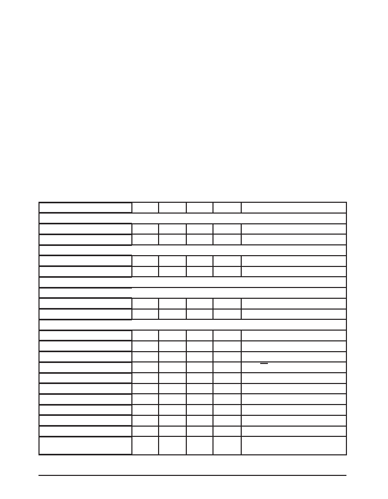
ABSOLUTE MAXIMUM RATINGS
These are stress ratings only and functional operation
of the device at these ratings or any other above those
indicated in the operation sections of the specifications
below is not implied. Exposure to absolute maximum
rating conditions for extended periods of time may
affect reliability.
V
CC.......................................................................+7V
Input Voltages:
Logic...........................-0.3V to (V
CC+0.5V)
Drivers........................-0.3V to (V
CC+0.5V)
Receivers..........................................±5V
Output Voltages:
Logic...........................-0.3V to (V
CC+0.5V)
Drivers...............................................±4V
Receivers....................-0.3V to (V
CC+0.5V)
Storage Temperature.......................-65C to +150C
Power Dissipation.......................................2000mW
Package Derating:
JA................................................46 °C/W
JC................................................6 °C/W
STORAGE CONSIDERATIONS
Due to the relatively large package size of the 80-pin
quad flat-pack, storage in a low humidity environment
is preferred. Large high density plastic packages
are moisture sensitive and should be stored in Dry
Vapor Barrier Bags. Prior to usage, the parts should
remain bagged and stored below 40°C and 60%RH.
If the parts are removed from the bag, they should be
used within 48 hours or stored in an environment at
or below 20%RH. If the above conditions cannot be
followed, the parts should be baked for four hours at
25°C in order remove moisture prior to soldering.
Exar ships the 80-pin QFP in Dry Vapor Barrier Bags
with a humidity indicator card and desiccant pack.The
humidity indicator should be below 30%RH.
SPECIFICATIONS
T
A = +25°C and VCC = +5.0V unless otherwise noted.
PARAMETER
MIN.
TYP.
MAX.
UNITS CONDITIONS
Logic Inputs
V
IL
0.8
Volts
V
IH
2.0
Volts
LOGIC OUTPUTS
V
OL
0.4
Volts
I
OUT = +3.2mA
V
OH
2.4
Volts
I
OUT = -.0mA
RS-485 DRIVER
TTL Input Levels
V
IL
0.8
Volts
V
IH
2.0
Volts
Outputs
HIGH Level Output
+6.0
Volts
LOW Level Output
-0.3
Volts
Differential Output
+/-.5
+/-5.0
Volts
R
L = 54, CL = 50pF
Balance
+/-0.2
Volts
|V
T| - |VT|
Offset
+2.5
Volts
Open Circuit Voltage
+/-6.0
Volts
Output Current
28.0
mA
R
L = 54
Short-Circuit Current
+/-250
mA
Terminated in -7V to +0V
Transition Time
20
40
ns
Rise/Fall time, 0% to 90%
Max. Transmission Rate
0
Mbps
R
L = 54; Figure 3a
Propagation Delay t
PHL
50
80
00
ns
T
A @ 25°C and VCC = +5V only Fig-
ures 3a and 5; R
L= 54, CL=50pF
相關(guān)PDF資料 |
PDF描述 |
|---|---|
| SP505BCM-L | IC TXRX WAN MULTI-MODE 80LQFP |
| SP506CM-L | IC TXRX WAN MULTI-MODE 80LQFP |
| SP507CM-L | IC TXRX WAN MULTI-MODE 80LQFP |
| SP508EF-L | IC TXRX MULTIPROTOCOL 100LQFP |
| SP510CM-L | IC TXRX MULTIPROTOCOL HS 100LQFP |
相關(guān)代理商/技術(shù)參數(shù) |
參數(shù)描述 |
|---|---|
| SP504MCM-L/TR | 功能描述:LIN 收發(fā)器 WAN Multi-Mode Serial Transceiver RoHS:否 制造商:NXP Semiconductors 工作電源電壓: 電源電流: 最大工作溫度: 封裝 / 箱體:SO-8 |
| SP505 | 制造商:EXAR 制造商全稱:EXAR 功能描述:WAN Multi-Mode Serial Transceiver |
| SP5054 | 制造商:MITEL 制造商全稱:Mitel Networks Corporation 功能描述:2.6GHz 3-Wire BUS Controlled Synthesiser |
| SP5054KGDPAS | 制造商:MITEL 制造商全稱:Mitel Networks Corporation 功能描述:2.6GHz 3-Wire BUS Controlled Synthesiser |
| SP5054SKGMPAS | 制造商:MITEL 制造商全稱:Mitel Networks Corporation 功能描述:2.6GHz 3-Wire BUS Controlled Synthesiser |
發(fā)布緊急采購,3分鐘左右您將得到回復(fù)。