- 您現(xiàn)在的位置:買賣IC網(wǎng) > PDF目錄98080 > SI5374B-A-GL (SILICON LABORATORIES) 808 MHz, PROC SPECIFIC CLOCK GENERATOR, PBGA80 PDF資料下載
參數(shù)資料
| 型號: | SI5374B-A-GL |
| 廠商: | SILICON LABORATORIES |
| 元件分類: | 時鐘產(chǎn)生/分配 |
| 英文描述: | 808 MHz, PROC SPECIFIC CLOCK GENERATOR, PBGA80 |
| 封裝: | 10 X 10 MM, ROHS COMPLIANT, PLASTIC, MO-192, BGA-80 |
| 文件頁數(shù): | 6/64頁 |
| 文件大小: | 303K |
| 代理商: | SI5374B-A-GL |
第1頁第2頁第3頁第4頁第5頁當前第6頁第7頁第8頁第9頁第10頁第11頁第12頁第13頁第14頁第15頁第16頁第17頁第18頁第19頁第20頁第21頁第22頁第23頁第24頁第25頁第26頁第27頁第28頁第29頁第30頁第31頁第32頁第33頁第34頁第35頁第36頁第37頁第38頁第39頁第40頁第41頁第42頁第43頁第44頁第45頁第46頁第47頁第48頁第49頁第50頁第51頁第52頁第53頁第54頁第55頁第56頁第57頁第58頁第59頁第60頁第61頁第62頁第63頁第64頁
Si5374
14
Preliminary Rev. 0.4
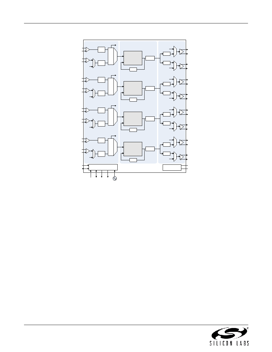
3. Functional Description
Figure 3. Functional Block Diagram
The Si5374 is a highly integrated jitter-attenuating clock multiplier that integrates four fully independent DSPLLs
and provides ultra-low jitter generation with less than 400 fs RMS. Configuration and control of the Si5374 is mainly
handled through the I2C interface. The device accepts clock inputs ranging from 2 kHz to 710 MHz and generates
independent, synchronous clock outputs ranging from 2 kHz to 808 MHz for each DSPLL. Virtually any frequency
translation (M/N) combination across its operating range is supported. The Si5374 supports a digitally
programmable loop bandwidth that can range from 4 to 525 Hz requiring no external DSPLL components. An
external single-ended or differential reference clock or XO is required for the device to enable ultra-low jitter
generation and jitter attenuation.
The device monitors each input clock for loss-of-signal (LOS) and provides a LOS alarm when missing pulses on
any of the input clocks are detected. The device monitors the lock status of each DSPLL and provides a Loss-of-
Lock (LOL) alarm when the DSPLL is unlocked. The lock detect algorithm continuously monitors the phase of the
selected input clock in relation to the phase of the feedback clock. The Si5374 provides a holdover capability that
allows the device to continue generation of a stable output clock when the input reference is lost. The reference
oscillator can be internally routed into CKIN2_q, so free-running clock generation is supported for each DSPLL
offering simultaneous synchronous and asynchronous operation.
The output drivers are configurable to support common signal formats, such as LVPECL, LVDS, CML, and CMOS
loads. If the CMOS signal format is selected, each differential output buffer generates two in-phase CMOS clocks
at the same frequency. For system-level debugging, a DSPLL bypass mode drives the clock output directly from
the selected input clock, bypassing the internal DSPLL.
Silicon Laboratories offers a PC-based software utility, DSPLLsim that can be used to determine valid frequency
plans and loop bandwidth settings to simplify device setup. DSPLLsim provides the optimum input, output, and
feedback divider values for a given input frequency and clock multiplication ratio that minimizes phase noise. This
utility can be downloaded from http://www.silabs.com/timing. For further assistance, refer to the Si53xx Any-
CKIN3P_B
CKOUT3N_B
÷ N31
DSPLL
B
÷ NC1
÷ NC2
CKIN3N_B
CKIN4P_B
÷ N32
CKIN4N_B
Internal
Osc
PLL Bypass
CKOUT3P_B
CKOUT4N_B
CKOUT4P_B
fOSC
÷ NC1_HS
Input
Monitor
Hitless
Switch
PLL Bypass
f3
÷ N2
Status / Control
PLL Bypass
High PSRR
Voltage Regulator
VDD_q
GND
Synthesis Stage
CKIN1P_A
CKOUT1N_A
÷ N31
DSPLL
A
÷ NC1
÷ NC2
CKIN1N_A
CKIN2P_A
÷ N32
CKIN2N_A
Internal
Osc
PLL Bypass
CKOUT1P_A
CKOUT2N_A
CKOUT2P_A
Output Stage
fOSC
÷ NC1_HS
Input
Monitor
Hitless
Switch
PLL Bypass
f3
÷ N2
PLL Bypass
Input Stage
CKIN7P_D
CKOUT7N_D
÷ N31
DSPLL
D
÷ NC1
÷ NC2
CKIN7N_D
CKIN8P_D
÷ N32
CKIN8N_D
Internal
Osc
PLL Bypass
CKOUT7P_D
CKOUT8N_D
CKOUT8P_D
fOSC
÷ NC1_HS
Input
Monitor
Hitless
Switch
PLL Bypass
f3
÷ N2
PLL Bypass
CKIN5P_C
CKOUT5N_C
÷ N31
DSPLL
C
÷ NC1
÷ NC2
CKIN5N_C
CKIN6P_C
÷ N32
CKIN6N_C
Internal
Osc
PLL Bypass
CKOUT5P_C
CKOUT6N_C
CKOUT6P_C
fOSC
÷ NC1_HS
Input
Monitor
Hitless
Switch
PLL Bypass
f3
÷ N2
PLL Bypass
RSTL_q
CS_CA_q
SCL
SDA LOL_q IRQ_q
Low Jitter
XO or Clock
OSC_P/N
相關(guān)PDF資料 |
PDF描述 |
|---|---|
| SI5375B-A-GL | 808 MHz, PROC SPECIFIC CLOCK GENERATOR, PBGA80 |
| SII0680A | IDE COMPATIBLE, CD ROM CONTROLLER, PQFP144 |
| SII3114CT176 | PCI BUS CONTROLLER, PQFP176 |
| SII3114CTU | PCI BUS CONTROLLER, PQFP176 |
| SII3124ACBHU | PCI BUS CONTROLLER, PBGA364 |
相關(guān)代理商/技術(shù)參數(shù) |
參數(shù)描述 |
|---|---|
| Si5374-EVB | 功能描述:時鐘和定時器開發(fā)工具 QUAD DSPLL 8IN/8OUT CLOCK EVAL KIT RoHS:否 制造商:Texas Instruments 產(chǎn)品:Evaluation Modules 類型:Clock Conditioners 工具用于評估:LMK04100B 頻率:122.8 MHz 工作電源電壓:3.3 V |
| Si5375B-A-BL | 功能描述:時鐘合成器/抖動清除器 Loop BW 60Hz-8.4 kHz 4In/Out 2kHz-808MHz RoHS:否 制造商:Skyworks Solutions, Inc. 輸出端數(shù)量: 輸出電平: 最大輸出頻率: 輸入電平: 最大輸入頻率:6.1 GHz 電源電壓-最大:3.3 V 電源電壓-最小:2.7 V 封裝 / 箱體:TSSOP-28 封裝:Reel |
| Si5375B-A-GL | 功能描述:時鐘合成器/抖動清除器 QUAD DSPLL JITT ATT CLK ST LP BW 4IN/OUT RoHS:否 制造商:Skyworks Solutions, Inc. 輸出端數(shù)量: 輸出電平: 最大輸出頻率: 輸入電平: 最大輸入頻率:6.1 GHz 電源電壓-最大:3.3 V 電源電壓-最小:2.7 V 封裝 / 箱體:TSSOP-28 封裝:Reel |
| Si5375-EVB | 功能描述:時鐘和定時器開發(fā)工具 QUAD DSPLL 4IN/4OUT CLOCK EVAL KIT RoHS:否 制造商:Texas Instruments 產(chǎn)品:Evaluation Modules 類型:Clock Conditioners 工具用于評估:LMK04100B 頻率:122.8 MHz 工作電源電壓:3.3 V |
| SI5376B-A-BL | 制造商:Silicon Laboratories Inc 功能描述:QUAD DSPLL JITTER ATTENUATING CLOCK, - Trays 制造商:Silicon Laboratories Inc 功能描述:IC CLK GEN/JITTER ATTEN 80PBGA |
發(fā)布緊急采購,3分鐘左右您將得到回復。