- 您現(xiàn)在的位置:買賣IC網(wǎng) > PDF目錄374768 > SED1335F (Electronic Theatre Controls, Inc.) LCD Controller ICs PDF資料下載
參數(shù)資料
| 型號(hào): | SED1335F |
| 廠商: | Electronic Theatre Controls, Inc. |
| 英文描述: | LCD Controller ICs |
| 中文描述: | LCD控制器芯片 |
| 文件頁數(shù): | 22/148頁 |
| 文件大?。?/td> | 388K |
| 代理商: | SED1335F |
第1頁第2頁第3頁第4頁第5頁第6頁第7頁第8頁第9頁第10頁第11頁第12頁第13頁第14頁第15頁第16頁第17頁第18頁第19頁第20頁第21頁當(dāng)前第22頁第23頁第24頁第25頁第26頁第27頁第28頁第29頁第30頁第31頁第32頁第33頁第34頁第35頁第36頁第37頁第38頁第39頁第40頁第41頁第42頁第43頁第44頁第45頁第46頁第47頁第48頁第49頁第50頁第51頁第52頁第53頁第54頁第55頁第56頁第57頁第58頁第59頁第60頁第61頁第62頁第63頁第64頁第65頁第66頁第67頁第68頁第69頁第70頁第71頁第72頁第73頁第74頁第75頁第76頁第77頁第78頁第79頁第80頁第81頁第82頁第83頁第84頁第85頁第86頁第87頁第88頁第89頁第90頁第91頁第92頁第93頁第94頁第95頁第96頁第97頁第98頁第99頁第100頁第101頁第102頁第103頁第104頁第105頁第106頁第107頁第108頁第109頁第110頁第111頁第112頁第113頁第114頁第115頁第116頁第117頁第118頁第119頁第120頁第121頁第122頁第123頁第124頁第125頁第126頁第127頁第128頁第129頁第130頁第131頁第132頁第133頁第134頁第135頁第136頁第137頁第138頁第139頁第140頁第141頁第142頁第143頁第144頁第145頁第146頁第147頁第148頁
S-MOS Systems, Inc. 2460 North First Street San Jose, CA 95131 Tel: (408) 922-0200 Fax: (408) 922-0238
22
268-0.4
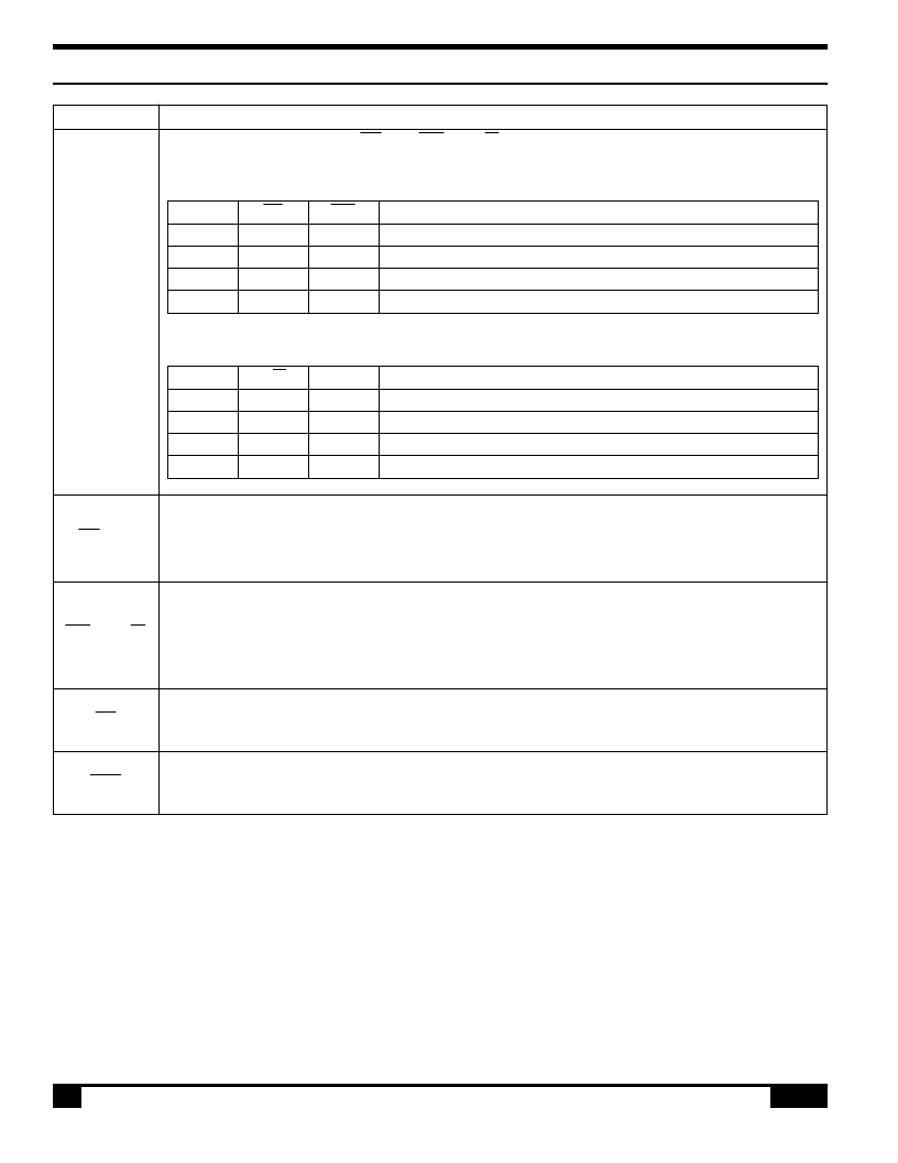
2.0 Pin Description
2.4.3
Pin Name
Function
A0, in conjunction with the RD and WR or R/W and E signals, controls the type of access to
the SED1336F, as shown below.
8080 family interface
A0
0
1
0
1
RD
0
0
1
1
WR
1
1
0
0
Function
Status flag read
Display data and cursor address read
Display data and parameter write
Command write
6800 family interface
A0
0
1
0
1
R/W
1
1
0
0
E
1
1
1
1
Function
Status flag read
Display data and cursor address read
Display data and parameter write
Command write
When the 8080 family interface is selected, this signal acts as the active-LOW read strobe. The
SED1330F/1335F/1336F’s output buffers are enabled when this signal is active.
When the 6800 family interface is selected, this signal acts as the active-HIGH enable clock.
Data is read from or written to the SED1330F/1335F/1336F when this clock goes HIGH.
When the 8080 family interface is selected, this signal acts as the active-LOW write strobe. The
bus data is latched on the rising edge of this signal.
When the 6800 family interface is selected, this signal acts as the read/write control signal. Data
is read from the SED1330F/1335F/1336F if this signal is HIGH, and written to the SED1330F/
1335F/1336F if it is LOW.
Chip select. This active-LOW input enables the SED1330F/1335F/1336F. It is usually
connected to the output of an address decoder device that maps the SED1330F/1335F/1336F
into the memory space of the controlling microprocessor.
This active-LOW input performs a hardware reset on the SED1330F/1335F/1336F. It is a
Schmitt-trigger input for enhanced noise immunity; however, care should be taken to ensure
that it is not triggered if the supply voltage is lowered.
WR or R/W
CS
RES
RD or E
A0
相關(guān)PDF資料 |
PDF描述 |
|---|---|
| SED1336F | LCD Controller ICs |
| SED1500 | DOT MATRIX LCD DRIVER |
| SED1501 | DOT MATRIX LCD DRIVER |
| SED1502 | DOT MATRIX LCD DRIVER |
| SED1503 | DOT MATRIX LCD DRIVER |
相關(guān)代理商/技術(shù)參數(shù) |
參數(shù)描述 |
|---|---|
| SED1335F0A | 制造商:EPSON 制造商全稱:EPSON 功能描述:LCD Controller ICs |
| SED1335F0B | 制造商:EPSON 制造商全稱:EPSON 功能描述:LCD Controller ICs |
| SED1335FOA | 功能描述:LCD 驅(qū)動(dòng)器 SMOS Controller Chip RoHS:否 制造商:Maxim Integrated 數(shù)位數(shù)量:4.5 片段數(shù)量:30 最大時(shí)鐘頻率:19 KHz 工作電源電壓:3 V to 3.6 V 最大工作溫度:+ 85 C 最小工作溫度:- 20 C 封裝 / 箱體:PDIP-40 封裝:Tube |
| SED1336 | 制造商:未知廠家 制造商全稱:未知廠家 功能描述:CMOS GRAPHIC LCD/TV CONTROLLER |
| SED1336F | 制造商:未知廠家 制造商全稱:未知廠家 功能描述:LCD Controller ICs |
發(fā)布緊急采購,3分鐘左右您將得到回復(fù)。