- 您現(xiàn)在的位置:買賣IC網(wǎng) > PDF目錄374727 > SC415 (Semtech Corporation) Dual Synchronous Buck Controller PDF資料下載
參數(shù)資料
| 型號: | SC415 |
| 廠商: | Semtech Corporation |
| 英文描述: | Dual Synchronous Buck Controller |
| 中文描述: | 雙同步降壓控制器 |
| 文件頁數(shù): | 22/30頁 |
| 文件大?。?/td> | 942K |
| 代理商: | SC415 |
第1頁第2頁第3頁第4頁第5頁第6頁第7頁第8頁第9頁第10頁第11頁第12頁第13頁第14頁第15頁第16頁第17頁第18頁第19頁第20頁第21頁當(dāng)前第22頁第23頁第24頁第25頁第26頁第27頁第28頁第29頁第30頁
SC415
22
Layout Guidelines
As with any switch-mode converter, and especially a
dual-channel converter, a good pcb layout is essential for
optimum performance. The following guidelines should
be used for pcb layout.
Placement
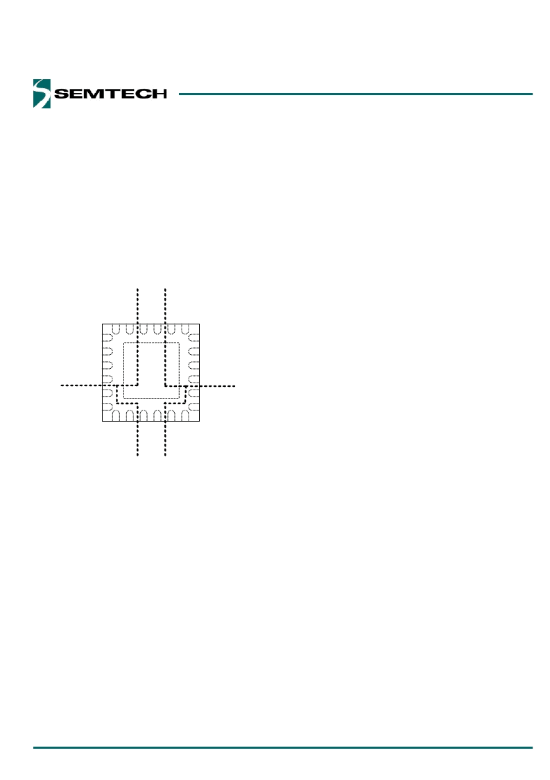
Note that the pins on the IC are arranged in four groups,
i.e. Side1 Power, Side2 Power, Side1 Analog, and Side2
Analog, as shown below.
LX1
BST1
VDD1
DL1
EN1
SS1
LX2
BST2
VDD2
DL2
EN2
SS2
D
I
P
P
I
D
V
F
R
T
F
V
GND
(PAD)
1
7
6
12
13
18
19
24
SC415
Side 1
Power/Gate
Drive
Side 2
Power/Gate
Drive
Side 1
Analog
Side 2
Analog
Figure 17
For placement, power devices for side1 should be grouped
together near the gate drive pins for side1 (pins 23-24 and
1-8). Power devices for side2 should be grouped together
near the gate-drive pins for side2 (pins 15-20).
The feedback and VOUT sense components should
be located near the FBx/VOUTx pins. This includes the
feedback resistors and capacitors if used.
Ground Connections
When doing placement, be aware that there are four
grounds.
Power ground for Side1
Power ground for Side2
Analog ground for Side1
Analog ground for Side2
Note that grounds (1) and (2) are high-current and contain
high noise. These grounds carry the DL gate drive current
as well as the high switching current through the MOSFETs
and low-side diode. It is important to note that the SC415
has only one power ground pin (PAD, pin 25), which must
drive DL for both side1 and side2. As such, the low-side
MOSFET and diode will need to be near the IC.
Grounds (3) and (4) are low-current and intended for low-
noise VOUT/FB ripple sensing. Note that there is only one
analog ground pin (RTN, pin 9) which shared between
sides 1 and 2.
Proper connection between the grounds is needed
for good operation. Generally, all ground connections
between the power components and the SC415 should
be short and direct, without vias where possible. Each
side has significant high-current switching in the ground
path, moving between the input capacitors, the low-
side MOSFET, the low-side diode if used, and the output
capacitors. Moreover, each side has significant high-
current pulses to/from the ground PAD, created by the DL
drive to the low-side MOSFETs. The DL gate-drive current
peaks can be 2 amps or more, with fast switching. As such
the ground connection between the low-side MOSFETs
and the ground PAD should be as short and wide as
practical.
Note that the ground PAD, which is the return path for
the high-noise DL drive current, is not accessible on the
top layer of the pcb, due to the other pins. The ground
1.
2.
3.
4.
Applications Information (continued)
相關(guān)PDF資料 |
PDF描述 |
|---|---|
| SC415EVB | Dual Synchronous Buck Controller |
| SC415MLTRT | Dual Synchronous Buck Controller |
| SC416 | Dual Synchronous Buck Controller with Tracking Start-up/Shutdown |
| SC416EVB | Dual Synchronous Buck Controller with Tracking Start-up/Shutdown |
| SC416MLTRT | Dual Synchronous Buck Controller with Tracking Start-up/Shutdown |
相關(guān)代理商/技術(shù)參數(shù) |
參數(shù)描述 |
|---|---|
| SC415_08 | 制造商:SEMTECH 制造商全稱:Semtech Corporation 功能描述:Dual Synchronous Buck Controller |
| SC4150 | 制造商:SEMTECH 制造商全稱:Semtech Corporation 功能描述:Negative Voltage Hot Swap Controller |
| SC4150HIS-4TRT | 制造商:SEMTECH 制造商全稱:Semtech Corporation 功能描述:Negative Voltage Hot Swap Controller |
| SC4150HISTRT | 制造商:SEMTECH 制造商全稱:Semtech Corporation 功能描述:Negative Voltage Hot Swap Controller |
| SC4150LIS-4TRT | 制造商:SEMTECH 制造商全稱:Semtech Corporation 功能描述:Negative Voltage Hot Swap Controller |
發(fā)布緊急采購,3分鐘左右您將得到回復(fù)。