- 您現(xiàn)在的位置:買賣IC網(wǎng) > PDF目錄385815 > SBDIP (Intersil Corporation) High-Reliability CMOS 8-Bit Microprocessor PDF資料下載
參數(shù)資料
| 型號: | SBDIP |
| 廠商: | Intersil Corporation |
| 英文描述: | High-Reliability CMOS 8-Bit Microprocessor |
| 中文描述: | 高可靠性的CMOS 8位微處理器 |
| 文件頁數(shù): | 3/8頁 |
| 文件大小: | 44K |
| 代理商: | SBDIP |
3-32
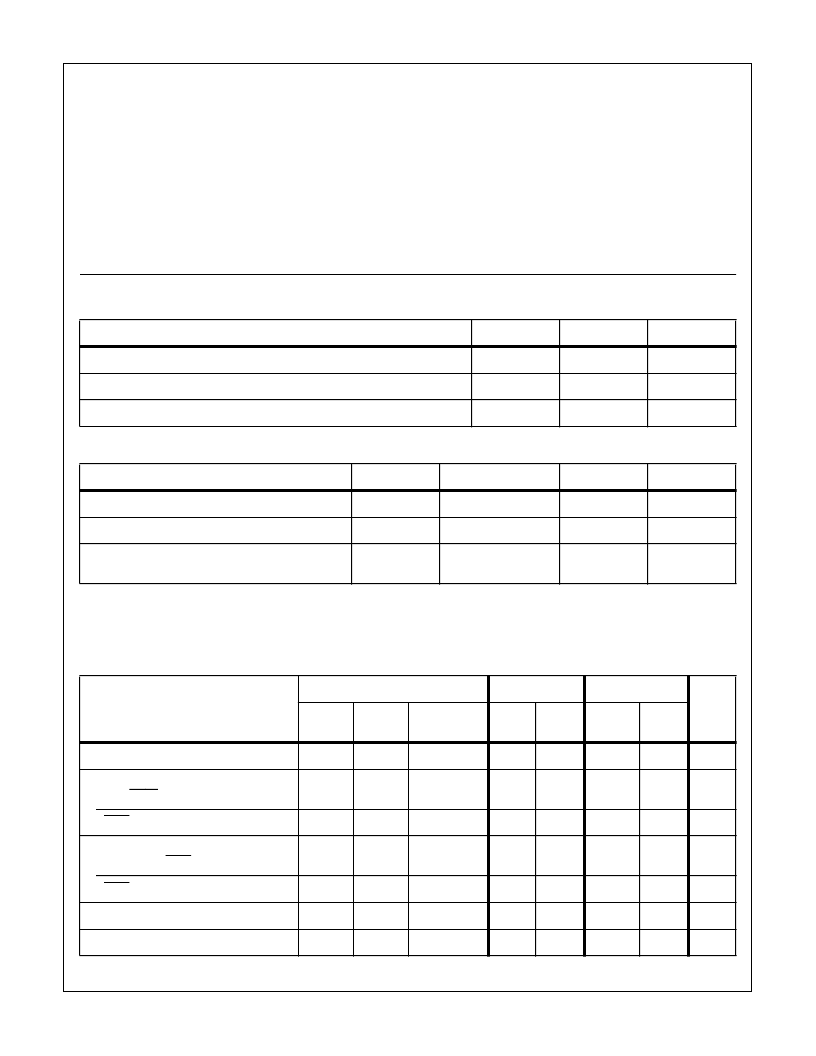
Absolute Maximum Ratings
Thermal Information
DC Supply Voltage Range, (V
DD
)
(All Voltages Referenced to V
SS
Terminal)
CDP1802AC/3 . . . . . . . . . . . . . . . . . . . . . . . . . . . . . . -0.5V to +7V
Input Voltage Range, All Inputs . . . . . . . . . . . . . -0.5V to V
DD
+0.5V
DC Input Current, any One Input
. . . . . . . . . . . . . . . . . . . . . . . . .±
10mA
Thermal Resistance (Typical)
SBDIP Package. . . . . . . . . . . . . . . . . . . .
Device Dissipation Per Output Transistor
T
A
= Full Package Temperature Range. . . . . . . . . . . . . . . . . 100mW
Operating Temperature Range (T
A
)
Package Type D. . . . . . . . . . . . . . . . . . . . . . . . . .-55
o
C to +125
o
C
Storage Temperature Range (T
STG
). . . . . . . . . . . .-65
o
C to +150
o
C
Lead Temperature (During Soldering)
At distance 1/16
±
1/32 In. (1.59
±
0.79mm)
from case for 10s max . . . . . . . . . . . . . . . . . . . . . . . . . . .+265
o
C
θ
JA
(
o
C/W)
55
θ
JC
(
o
C/W)
15
CAUTION: Stresses above those listed in “Absolute Maximum Ratings” may cause permanent damage to the device. This is a stress only rating and operation
of the device at these or any other conditions above those indicated in the operational sections of this specification is not implied.
Recommended Operating Conditions
T
A
= Full Package Temperature Range. For maximum reliability, operating conditions
should be selected so that operation is always within the following ranges
PARAMETER
MIN
MAX
UNITS
DC Operating Voltage Range
4
6.5
V
Input Voltage Range
V
SS
V
DD
V
Maximum Clock Input Rise or Fall Time
-
1
μ
s
Performance Specifications
PARAMETER
V
DD
(V)
-
55
o
C TO +25
o
C
+125
o
C
UNITS
Minimum Instruction Time (Note 1)
5
4.5
5.9
μ
s
Maximum DMA Transfer Rate
5
450
340
Kbytes/s
Maximum Clock Input Frequency,
Load Capacitance (C
L
) = 50pF, f
CL
5
DC-3.6
DC-2.7
MHz
NOTE:
1. Equals 2 machine cycles - one Fetch and one Execute operation for all instructions except Long Branch and Long Skip, which require 3
machine cycles - one Fetch and two Execute operations.
Static Electrical Specifications
All Limits are 100% Tested
PARAMETER
CONDITIONS
-55
o
C, +25
o
C
+125
o
C
UNITS
V
OUT
(V)
V
IN,
(V)
V
CC,
V
DD
(V)
MIN
MAX
MIN
MAX
Quiescent Device Current, I
DD
-
-
5
-
100
-
250
μ
A
Output Low Drive (Sink) Current
(Except XTAL), I
OL
0.4
0, 5
5
1.20
-
0.90
-
mA
XTAL
0.4
5
5
185
-
140
-
μ
A
Output High Drive (Source)
Current (Except XTAL), I
OH
4.6
0, 5
5
-
-0.30
-
-0.20
mA
XTAL
4.6
0
5
-
-135
-
-100
μ
A
Output Voltage Low-Level, V
OL
-
0, 5
5
-
0.1
-
0.2
V
Output Voltage High-Level, V
OH
-
0, 5
5
4.9
-
4.8
-
V
CDP1802AC/3
相關(guān)PDF資料 |
PDF描述 |
|---|---|
| SBR12040 | 120 AMP SCHOTTKY RECTIFIER |
| SBR12045 | 120 AMP SCHOTTKY RECTIFIER |
| SBR12050 | 120 AMP SCHOTTKY RECTIFIER |
| SBR2530 | 25 Amp Schottky Rectifier |
| SBR2535 | TP Series Rocker Switch, 1 pole, 3 position, Screw terminal, Flush Panel Mounting |
相關(guān)代理商/技術(shù)參數(shù) |
參數(shù)描述 |
|---|---|
| SBDL1 | 制造商:Banner Engineering 功能描述:Sensor, Photoelectric, Diffuse, 0.6 Meter Range, 3/4 Wire Scanner Block 制造商:Banner Engineering 功能描述:PHOTOELECTRIC SENSOR; Sensing Range Max:600mm; Range:24"; Sensing Range:0mm to 600mm; Sensor Housing:Rectangular; Sensor Input:Optical; Series:MULTI-BEAM; Turn Off Time:1ms; Turn On Time:1ms ;RoHS Compliant: Yes |
| SBDR-1201-1B | 制造商:DEC 制造商全稱:DEC 功能描述:12 AMP SCHOTTKY BARRIER RECTIFIERS |
| SBDR-1601-1B | 制造商:DEC 制造商全稱:DEC 功能描述:16 AMP SCHOTTKY BARRIER RECTIFIERS |
| SBDR-601-1B | 制造商:DEC 制造商全稱:DEC 功能描述:6 AMP SCHOTTKY BARRIER RECTIFIERS |
| SB-DS75LC | 制造商:TOKO Inc XXX 功能描述:Design kit SMD Inductors DS75LC range |
發(fā)布緊急采購,3分鐘左右您將得到回復(fù)。