- 您現(xiàn)在的位置:買賣IC網(wǎng) > PDF目錄359286 > S3901-1024Q (Hamamatsu Photonics) NMOS Linear image sensor PDF資料下載
參數(shù)資料
| 型號: | S3901-1024Q |
| 廠商: | Hamamatsu Photonics |
| 英文描述: | NMOS Linear image sensor |
| 中文描述: | NMOS管線性圖像傳感器 |
| 文件頁數(shù): | 2/4頁 |
| 文件大?。?/td> | 122K |
| 代理商: | S3901-1024Q |
NMOS linear image sensor
S3901-1024Q, S3904-2048Q
I
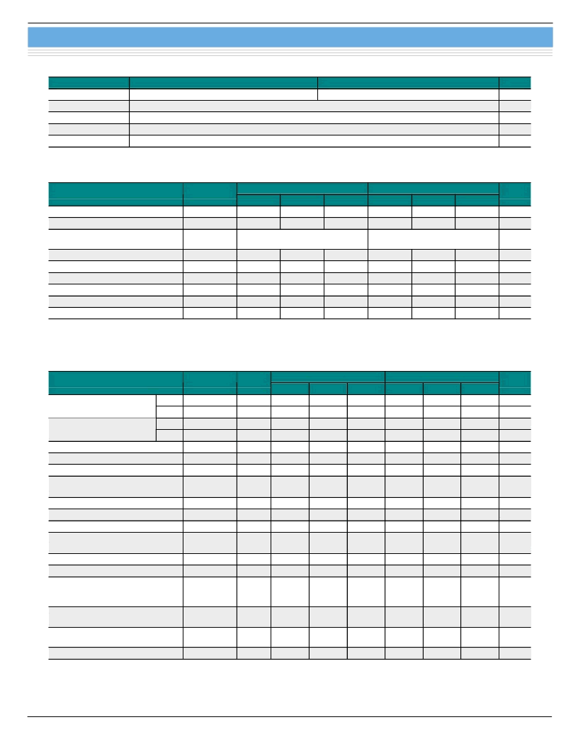
Shape specifications
Parameter
Number of pixels
Package length
Number of pin
Window material *
3
Weight
*3: Fiber optic plate is available.
S3901-1024Q
1024
S3904-2048Q
2048
Unit
-
mm
-
-
g
65.0
22
Quartz
8.5
I
Specifications (Ta=25 °C)
S3901-1024Q
Typ.
50
2.5
S3904-2048Q
Typ.
25
2.5
Parameter
Symbol
Min.
-
-
Max.
-
-
Min.
-
-
Max.
-
-
Unit
Pixel pitch
Pixel height
Spectral response range
(10 % of peak)
Peak sensitivity wavelength
Photodiode dark current *
4
Photodiode capacitance *
4
Saturation exposure *
4,
*
5
Saturation output charge *
4
Photo response non-uniformity *
6
*4: Vb=2.0 V, V
φ
=5.0 V
*5: 2856 K, tungsten lamp
*6: 50 % of saturation, excluding the start pixel and last pixel
-
-
μm
mm
λ
200 to 1000
200 to 1000
nm
λ
p
I
D
Cph
Esat
Qsat
PRNU
-
-
-
-
-
-
600
0.2
20
180
50
-
-
-
-
-
-
-
-
600
0.1
10
180
25
-
-
nm
pA
pF
0.6
-
-
-
±3
0.3
-
-
-
±3
m
lx
·
s
pC
%
I
Electrical characteristics (Ta=25 °C)
S3901-1024Q
Typ.
5
-
V
φ
1
-
V
φ
- 3.0
0
Vb
S3904-2048Q
Typ.
5
-
V
φ
1
-
V
φ
- 3.0
0
Vb
Parameter
Symbol
Condition
Min.
4.5
0
4.5
0
1.5
-
-
Max.
10
0.4
10
0.4
V
φ
- 2.5
-
-
Min.
4.5
0
4.5
0
1.5
-
-
Max.
10
0.4
10
0.4
V
φ
- 2.5
-
-
Unit
High V
φ
1, V
φ
2 (H)
Low
V
φ
1, V
φ
2 (L)
High
V
φ
s (H)
Low
V
φ
s (L)
V
V
V
V
V
V
V
Clock pulse (
φ
1,
φ
2)
voltage
Start pulse (
φ
st) voltage
Video bias voltage *
7
Saturation control gate voltage
Saturation control drain voltage
Vb
Vscg
Vscd
tr
φ
1, tr
φ
2
tf
φ
1, tf
φ
2
tpw
φ
1, tpw
φ
2
tr
φ
s, tf
φ
s
tpw
φ
s
Clock pulse (
φ
1,
φ
2) rise/fall time
*
8
-
20
-
-
20
-
ns
Clock pulse (
φ
1,
φ
2) pulse width
Start pulse (
φ
st) rise/fall time
Start pulse (
φ
st) pulse width
Start pulse (
φ
st) and clock pulse
(
φ
2) overlap
Clock pulse space *
8
Data rate *
9
200
-
200
-
-
-
-
200
-
200
-
-
-
-
ns
ns
ns
20
-
20
-
t
φ
ov
200
-
-
200
-
-
ns
X
1
, X
2
f
trf - 20
0.1
-
-
-
trf - 20
0.1
-
-
-
ns
kHz
2000
2000
Video delay time
tvd
50 % of
saturation
*
9,
*
10
-
200
-
-
250
-
ns
Clock pulse (
φ
1,
φ
2)
line capacitance
Saturation control gate (Vscg)
line capacitance
Video line capacitance
*7: V
φ
is input pulse voltage (refer to figure 8) .
*8: trf is the clock pulse rise or fall time. A clock pulse space of
“rise time/fall time - 20
” ns (nanoseconds) or more should be
input if the clock pulse rise or fall time is longer than 20
*9: Vb=2.0 V, V
φ
=5.0 V
*10: Measured with C7883 driver circuit.
C
φ
5 V bias
-
134
-
-
200
-
pF
Cscg
5 V bias
-
63
-
-
87
-
pF
C
V
2 V bias
-
45
-
-
60
-
pF
ns (refer to figure 7) .
2
相關(guān)PDF資料 |
PDF描述 |
|---|---|
| S3901-512F | NMOS Linear image sensor |
| S3901 | NMOS Linear image sensor |
| S3901-128Q | NMOS Linear image sensor |
| S3901-256Q | NMOS Linear image sensor |
| S3901-512Q | NMOS Linear image sensor |
相關(guān)代理商/技術(shù)參數(shù) |
參數(shù)描述 |
|---|---|
| S3901-1024Q_07 | 制造商:HAMAMATSU 制造商全稱:Hamamatsu Corporation 功能描述:NMOS linear image sensor |
| S3901-128Q | 制造商:HAMAMATSU 制造商全稱:Hamamatsu Corporation 功能描述:NMOS Linear image sensor |
| S3901-2048Q | 制造商:HAMAMATSU 制造商全稱:Hamamatsu Corporation 功能描述:NMOS Linear image sensor |
| S3901-256F | 制造商:HAMAMATSU 制造商全稱:Hamamatsu Corporation 功能描述:NMOS linear image sensor |
| S3901-256Q | 制造商:HAMAMATSU 制造商全稱:Hamamatsu Corporation 功能描述:NMOS Linear image sensor |
發(fā)布緊急采購,3分鐘左右您將得到回復(fù)。