- 您現(xiàn)在的位置:買賣IC網(wǎng) > PDF目錄98068 > S1C63466D 4-BIT, MROM, 4.1 MHz, MICROCONTROLLER, UUC140 PDF資料下載
參數(shù)資料
| 型號: | S1C63466D |
| 元件分類: | 微控制器/微處理器 |
| 英文描述: | 4-BIT, MROM, 4.1 MHz, MICROCONTROLLER, UUC140 |
| 封裝: | DIE-140 |
| 文件頁數(shù): | 35/135頁 |
| 文件大小: | 1053K |
| 代理商: | S1C63466D |
第1頁第2頁第3頁第4頁第5頁第6頁第7頁第8頁第9頁第10頁第11頁第12頁第13頁第14頁第15頁第16頁第17頁第18頁第19頁第20頁第21頁第22頁第23頁第24頁第25頁第26頁第27頁第28頁第29頁第30頁第31頁第32頁第33頁第34頁當前第35頁第36頁第37頁第38頁第39頁第40頁第41頁第42頁第43頁第44頁第45頁第46頁第47頁第48頁第49頁第50頁第51頁第52頁第53頁第54頁第55頁第56頁第57頁第58頁第59頁第60頁第61頁第62頁第63頁第64頁第65頁第66頁第67頁第68頁第69頁第70頁第71頁第72頁第73頁第74頁第75頁第76頁第77頁第78頁第79頁第80頁第81頁第82頁第83頁第84頁第85頁第86頁第87頁第88頁第89頁第90頁第91頁第92頁第93頁第94頁第95頁第96頁第97頁第98頁第99頁第100頁第101頁第102頁第103頁第104頁第105頁第106頁第107頁第108頁第109頁第110頁第111頁第112頁第113頁第114頁第115頁第116頁第117頁第118頁第119頁第120頁第121頁第122頁第123頁第124頁第125頁第126頁第127頁第128頁第129頁第130頁第131頁第132頁第133頁第134頁第135頁
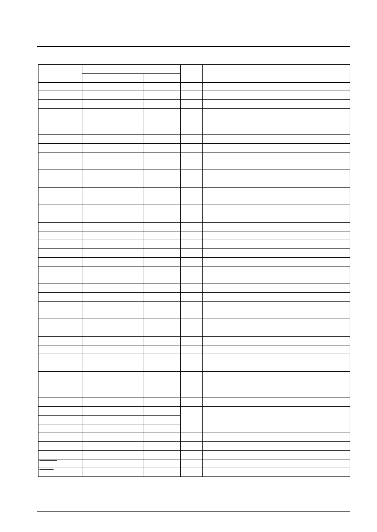
S1C63466 TECHNICAL MANUAL
EPSON
5
CHAPTER 1: OUTLINE
1.4 Pin Description
Table 1.4.1 Pin description
Pin name
VDD
VSS
VD1
VC1–VC5
VREF
CA–CF
OSC1
OSC2
OSC3
OSC4
K00–K03
K10, K11
K12
K13
P00–P03
P10–P13
P20
P21
P22
P23
R00
R01
R02
R03
R10–R13
R20–R23
COM0, COM1
COM2–COM14
COM15, COM16
SEG0–SEG59
BZ
SVD
RESET
TEST
QFP8-144,QFP17-144
31
25
28
75–79
34
85–80
26
27
29
30
70–67
66,65
64
63
62–59
58–55
54
53
52
51
50
49
48
47
46–43
42–39
23,22
21,20,18–15,86–92
93,94
14–1,143–110,106–95
24
74
32
33
QFP5-128
64
58
61
101–105
67
111–106
59
60
62
63
99–96
95,94
–
93
92–89
88–85
84
83
82
81
80
79
78
77
76–73
72–69
–
56–51,112–118
–
50–1,128–119
57
100
65
66
Function
Power (+) supply pin
Power (–) supply pin
Oscillation/internal logic system regulated voltage output pin
LCD system power supply pin
1/4 bias generated internally, 1/5 bias supplied externally
(selected by mask option)
LCD system power supply testing pin
LCD system boosting/reducing capacitor connecting pin
Crystal or CR oscillation input pin
(selected by mask option)
Crystal or CR oscillation output pin
(selected by mask option)
Ceramic or CR oscillation input pin
(selected by mask option)
Ceramic or CR oscillation output pin
(selected by mask option)
Input port
I/O port
(switching to serial I/F input/output is possible by software)
I/O port
(switching to CL signal output is possible by software)
I/O port
(switching to FR signal output is possible by software)
Output port
(switching to TOUT signal output is possible by software)
Output port
(switching to FOUT signal output is possible by software)
Output port
LCD common output pin
(1/8, 1/16, 1/17 duty can be selected by software)
LCD segment output pin
Sound output pin
SVD external voltage input pin
Initial reset input pin
Testing input pin
Pin No.
In/Out
–
O
–
I
O
I
O
I
I/O
O
I
相關PDF資料 |
PDF描述 |
|---|---|
| S1C63466F | 4-BIT, MROM, 4.1 MHz, MICROCONTROLLER, PQFP144 |
| S1C63567F0A0100 | MICROCONTROLLER, PQFP144 |
| S1C63653F | 4-BIT, FLASH, 4 MHz, MICROCONTROLLER, CQFP100 |
| S1C6F567D0A0100 | MICROCONTROLLER, UUC141 |
| S1C6N3B0D0A0100 | MICROCONTROLLER, UUC54 |
相關代理商/技術參數(shù) |
參數(shù)描述 |
|---|---|
| S1C63557D04Q000 | 制造商:Seiko Instruments Inc (SII) 功能描述:EPSON MCU 4BIT |
| S1C63567 | 制造商:EPSON 制造商全稱:EPSON 功能描述:4-bit Single Chip Microcomputer |
| S1C63616 | 制造商:EPSON 制造商全稱:EPSON 功能描述:4-bit Single Chip Microcomputer |
| S1C63632 | 制造商:EPSON 制造商全稱:EPSON 功能描述:4-bit Single Chip Microcomputer |
| S1C63653 | 制造商:EPSON 制造商全稱:EPSON 功能描述:CMOS 4-bit Single Chip Microcontroller |
發(fā)布緊急采購,3分鐘左右您將得到回復。