- 您現(xiàn)在的位置:買賣IC網(wǎng) > PDF目錄373275 > RK80532PC041512 Microprocessor PDF資料下載
參數(shù)資料
| 型號: | RK80532PC041512 |
| 英文描述: | Microprocessor |
| 中文描述: | 微處理器 |
| 文件頁數(shù): | 18/86頁 |
| 文件大小: | 882K |
| 代理商: | RK80532PC041512 |
第1頁第2頁第3頁第4頁第5頁第6頁第7頁第8頁第9頁第10頁第11頁第12頁第13頁第14頁第15頁第16頁第17頁當前第18頁第19頁第20頁第21頁第22頁第23頁第24頁第25頁第26頁第27頁第28頁第29頁第30頁第31頁第32頁第33頁第34頁第35頁第36頁第37頁第38頁第39頁第40頁第41頁第42頁第43頁第44頁第45頁第46頁第47頁第48頁第49頁第50頁第51頁第52頁第53頁第54頁第55頁第56頁第57頁第58頁第59頁第60頁第61頁第62頁第63頁第64頁第65頁第66頁第67頁第68頁第69頁第70頁第71頁第72頁第73頁第74頁第75頁第76頁第77頁第78頁第79頁第80頁第81頁第82頁第83頁第84頁第85頁第86頁
18
Datasheet
Intel
Pentium
III Processor with 512KB L2 Cache at 1.13GHz to 1.40GHz
2.6
Voltage Identification
There are five voltage identification (VID) pins on the PGA370 socket. These pins can be used to
support automatic selection of V
CCCORE
voltages. The VID pins for the Intel Pentium
III
processor with 512KB L2 Cache are open drain signals versus opens or shorts found on the
previous Intel
Pentium
III
processors in the FC-PGA package. Refer to
Table 11
for level
specifications for the VID signals. This pull-up resistor may be either external logic on the
motherboard or internal to the Voltage Regulator.
The VID signals rely on a 3.3V pull-up resistor to set the signal to a logic high level. The VID pins
are needed to fully support voltage specification variations on current and future processors. The
voltage selection range for the processor is defined in
Table 3
. The VID25mV signal is a new
signal that allows the voltage regulator or voltage regulator module (VRM) to output voltage levels
in 25mV increment necessary for the Intel Pentium
III
processor with 512KB L2 Cache only.
The legacy Pentium
III
processor in the FC-PGA package will not have this VID25mV signal.
The VID25mV pin location is actually a Vss pin on the Pentium
III
processor (CPUID = 068xh).
By connecting the VID25mV signal to the Vss pin, it will disable the 25mV stepping granularity
output and the regulator will resort to 50mV stepping increment. The voltage regulator or VRM
must supply the voltage that is requested or disable itself.
In addition to the new signal “VID25mV”, the Intel Pentium
III
processor with 512KB L2
Cache will introduce a second new signal labeled as “VTT_PWRGD”. The VTT_PWRGD signal
informs the platform that the VID and BSEL signals are stable and should be sampled. During
power-up, the VID signals will be in an indeterminate state for a small period of time. The voltage
regulator or the VRM should not latch the VID signals until the VTT_PWRGD signal is asserted
by the VRM and sampled active. The assertion of the VTT_PWRGD signal indicates the VID
signals are stable and are driven to the final state by the processor. Refer to
Figure 14
for power-up
timing sequence for the VTT_PWRGD and the VID signals.
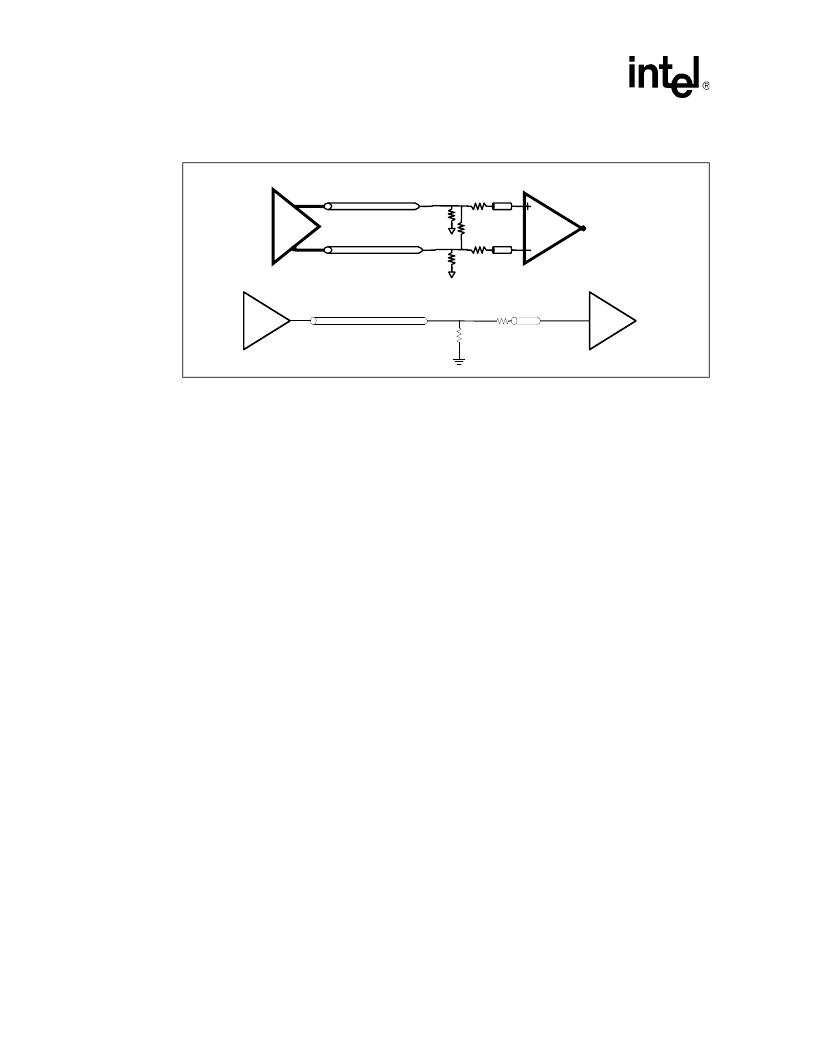
Figure 5. Differential/Single-Ended Clocking Example
BCLK
BCLK#
Clock
Driver
Processor or
Chipset
Clock
Driver
BCLK
Processor
orChipset
相關PDF資料 |
PDF描述 |
|---|---|
| RK9410 | TRANSISTOR | MOSFET | N-CHANNEL | 30V V(BR)DSS | 7A I(D) | SO |
| RKC-SERIES | Interface IC |
| RKCB-SERIES | Interface IC |
| RKCR-SERIES | Interface IC |
| RKCS-SERIES | Interface IC |
相關代理商/技術參數(shù) |
參數(shù)描述 |
|---|---|
| RK80532PC041512 SL5YR | 制造商:Intel 功能描述: |
| RK80532PC041512S L66R | 制造商:Intel 功能描述:MPU Pentium? 4 Processor 64-Bit 0.13um 2GHz 478-Pin FCPGA2 |
| RK80532PC041512S L6PK | 制造商:Intel 功能描述:MPU Pentium? 4 Processor 64-Bit 0.13um 2GHz 478-Pin FCPGA2 制造商:Intel 功能描述:32BIT MPU 80532PC041512 2G 512 - Trays 制造商:Intel 功能描述:NORTHWOOD; MPU PENTIUM 4 NETBURST 64BIT 0.13UM 2GHZ - Trays |
| RK80532PC041512SL6 | 制造商:Intel 功能描述:ITLRK80532PC041512SL6PK MPU MM#850362 |
| RK80532PC041512SL6PK | 制造商:Intel 功能描述:ITLRK80532PC041512SL6PK MM# 850362 / 32 |
發(fā)布緊急采購,3分鐘左右您將得到回復。