- 您現(xiàn)在的位置:買賣IC網(wǎng) > PDF目錄383737 > PC33926PNBR2 (飛思卡爾半導(dǎo)體(中國(guó))有限公司) 5.0 A Throttle Control H-Bridge PDF資料下載
參數(shù)資料
| 型號(hào): | PC33926PNBR2 |
| 廠商: | 飛思卡爾半導(dǎo)體(中國(guó))有限公司 |
| 英文描述: | 5.0 A Throttle Control H-Bridge |
| 中文描述: | 5.0甲節(jié)氣門控制H橋 |
| 文件頁數(shù): | 3/24頁 |
| 文件大?。?/td> | 378K |
| 代理商: | PC33926PNBR2 |
Analog Integrated Circuit Device Data
Freescale Semiconductor
3
33926
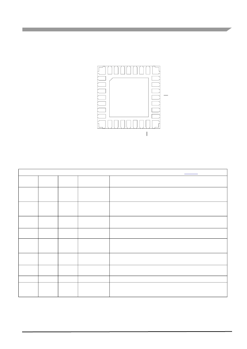
PIN CONNECTIONS
PIN CONNECTIONS
Figure 3. 33926 Pin Connections
Table 1. 33926 Pin Definitions
A functional description of each pin can be found in the Functional Description section beginning on
page 11
.
Pin
Pin Name
Pin
Function
Formal Name
Definition
1
IN2
Logic Input
Input 2
Logic input control of OUT2; e.g., when IN2 is logic HIGH, OUT2 is set to V
PWR
,
and when IN2 is logic LOW, OUT2 is set to PGND. (Schmitt trigger input with
~ 80
μ
A source so default condition = OUT2 HIGH.)
2
IN1
Logic Input
Input 1
Logic input control of OUT1; e.g., when IN1 is logic HIGH, OUT1 is set to V
PWR
,
and when IN1 is logic LOW, OUT1 is set to PGND. (Schmitt trigger Input with
~ 80
μ
A source so default condition = OUT1 HIGH.)
3
SLEW
Logic Input
Slew Rate
Logic input to select fast or slow slew rate. (Schmitt trigger input with ~ 80
μ
A
sink so default condition = slow.)
4, 6, 11, 31
VPWR
Power Input
Positive Power
Supply
These pins must be connected together physically as close as possible and
directly soldered down to a wide, thick, low resistance supply plane on the PCB.
5,
Exposed
Pad
AGND
Analog
Ground
Analog Signal
Ground
The low current analog signal ground must be connected to PGND via low
impedance path (<<10 m
, 0 Hz to 20 kHz). Exposed copper pad is also the
main heatsinking path for the device.
7
INV
Logic Input
Input Invert
Sets IN1 and IN2 to logic LOW = TRUE. (Schmitt trigger input with ~ 80
μ
A sink
so default condition = non-inverted.)
8
FB
Analog
Output
Feedback
Load current feedback output provides ground referenced 0.24% of H-Bridge
high-side output current. (Tie pin to GND through a resistor if not used.)
9, 17, 25
NC
No Connect
No internal connection is made to this pin.
10
EN
Logic Input
Enable Input
When EN is logic HIGH, the device is operational. When EN is logic LOW, the
device is placed in Sleep mode. (logic input with ~ 80
μ
A sink so default
condition = Sleep mode.)
Transparent Top
View of Package
25
17
18
19
20
21
22
23
24
9
10 11 12 13 14 15 16
1
2
3
4
5
6
7
8
26
27
28
29
30
31
32
NC
NC
V
NC
IN2
IN1
SLEW
O
AGND
INV
FB
E
O
VPWR
VPWR
O
O
AGND
O
D
PGND
SF
D
O
O
C
V
PGND
PGND
PGND
PGND
PGND
O
相關(guān)PDF資料 |
PDF描述 |
|---|---|
| PC33975A | Multiple Switch Detection Interface with Suppressed Wake-Up and 32mA Wetting Current |
| PC33975AEK | Multiple Switch Detection Interface with Suppressed Wake-Up and 32mA Wetting Current |
| PC33975AR2 | Multiple Switch Detection Interface with Suppressed Wake-Up and 32mA Wetting Current |
| PC3S12XEP100J1CAA | Microcontrollers |
| PC3S12XEP100J1CAAR | Microcontrollers |
相關(guān)代理商/技術(shù)參數(shù) |
參數(shù)描述 |
|---|---|
| PC33937APEK | 制造商:Freescale Semiconductor 功能描述: |
| PC33972ATEW | 制造商:Freescale Semiconductor 功能描述: |
| PC33975A | 制造商:FREESCALE 制造商全稱:Freescale Semiconductor, Inc 功能描述:Multiple Switch Detection Interface with Suppressed Wake-Up and 32mA Wetting Current |
| PC33975AEK | 制造商:FREESCALE 制造商全稱:Freescale Semiconductor, Inc 功能描述:Multiple Switch Detection Interface with Suppressed Wake-Up and 32mA Wetting Current |
| PC33975AR2 | 制造商:FREESCALE 制造商全稱:Freescale Semiconductor, Inc 功能描述:Multiple Switch Detection Interface with Suppressed Wake-Up and 32mA Wetting Current |
發(fā)布緊急采購,3分鐘左右您將得到回復(fù)。