- 您現(xiàn)在的位置:買(mǎi)賣(mài)IC網(wǎng) > PDF目錄1966 > QLX4300SIQSR (Intersil)IC EQUALIZER REC 3.125GBPS 46QFN PDF資料下載
參數(shù)資料
| 型號(hào): | QLX4300SIQSR |
| 廠商: | Intersil |
| 文件頁(yè)數(shù): | 7/21頁(yè) |
| 文件大小: | 0K |
| 描述: | IC EQUALIZER REC 3.125GBPS 46QFN |
| 標(biāo)準(zhǔn)包裝: | 100 |
| 系列: | QLx™ |
| 應(yīng)用: | 數(shù)據(jù)傳輸 |
| 接口: | SMBus(2 線/I²C) |
| 電源電壓: | 1.1 V ~ 1.3 V |
| 封裝/外殼: | 46-WFQFN 裸露焊盤(pán) |
| 供應(yīng)商設(shè)備封裝: | 46-TQFN |
| 包裝: | 帶卷 (TR) |
| 安裝類(lèi)型: | 表面貼裝 |
第1頁(yè)第2頁(yè)第3頁(yè)第4頁(yè)第5頁(yè)第6頁(yè)當(dāng)前第7頁(yè)第8頁(yè)第9頁(yè)第10頁(yè)第11頁(yè)第12頁(yè)第13頁(yè)第14頁(yè)第15頁(yè)第16頁(yè)第17頁(yè)第18頁(yè)第19頁(yè)第20頁(yè)第21頁(yè)
15
FN6982.1
November 19, 2009
Serial Bus Programming
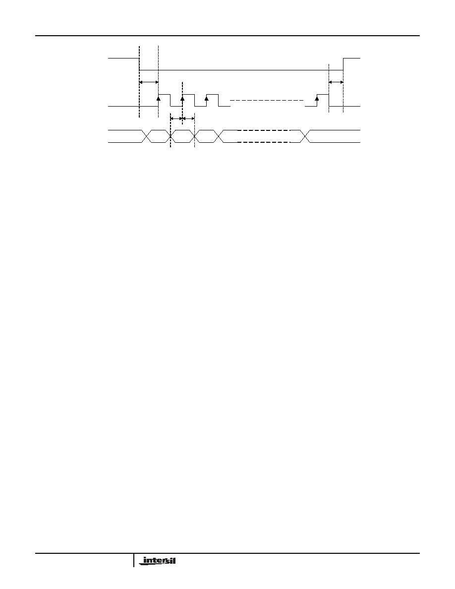
Pins 16 (DI), 45 (ENB), and 46 (CLK) are used to
program the registers inside the QLx4300-S45. Figure 22
shows an exemplary timing diagram for the signals on
these pins. The serial bus can be used to program a
single QLx4300-S45 according to the following steps:
1. The ENB pin is pulled ‘LOW’.
- While this pin is ‘LOW’, the data input on DI are
read into registers but not yet latched.
- A setup time of tSCK is needed between ENB going
‘LOW’ and the first rising clock edge.
2. At least 21 values are read from DI on the rising
edge of the CLK signal.
- If more than 21 values are passed in, then only the
last 21 values are kept in a FIFO fashion.
- The data on DI should start by sending the value
destined for register 21 and finish by sending the
value destined for register 1.
- A range of clock frequencies can be used. A typical
rate is 10MHz. The clock should not exceed 20MHz.
-Setup (tSDI) and hold (tHDI) times are needed
around the rising clock edge.
3. The ENB pin is pulled ‘HIGH’ and the contents of the
registers are latched and take effect.
- After clocking in the last data bit, an additional
tHEN should elapse before pulling the ENB signal
‘HIGH’.
- After completing these steps, the new values will
affect within tD.
Programming Multiple QLx4300-S45
Devices
The serial bus interface provides a simple means of
setting the equalizer boost levels with a minimal amount
of board circuitry. Many of the serial interface signals can
be shared among the QLx4300-S45 devices on a board
and two options are presented in this section. The first
uses common clock and serial data signals along with
separate ENB signals to select which QLx4300-S45
accepts the programmed changes. The second method
uses a common ENB signal as the serial data is
carried-over from one QLx4300-S45 to the next.
Separate ENB Signals
Multiple QLx4300-S45 devices can be programmed from
a common serial data stream as shown in Figure 23.
Here, each QLx4300-S45 is provided its own ENB signal,
and only one of these ENB signals is pulled ‘LOW’, and
hence accepting the register data one at a time. In this
situation, the programming of each equalizer follows the
steps outlined in Figure 22.
DI/DO Carryover
The DO pin (pin 17) can be used to daisy-chain the serial
bus among multiple QLx4300-S45 chips. The DO pin
outputs the overflow data from the DI pin. Specifically, as
data is pipelined into a QLx4300-S45, it proceeds
according to the following flow. First, a bit goes into
shadow register 1. Then, with each clock cycle, it shifts
over into subsequent higher numbered registers. After
shifting into register 21, it is output on the DO pin on the
same clock cycle. Thus, the DO signal is equal to the DI
signal, but delayed by 20 clock cycles. The timing
diagram for the DO pin is shown in Figure 24 where the
first 20 bits output from the DO are indefinite and
subsequent bits are the data fed into the DI pin. The
delay between the rising clock edge and the data
transition is tCQ.
A diagram for programming multiple QLx4300-S45s is
shown in Figure 25. It is noted that the board layout
should ensure that the additional clock delay experienced
between subsequent QLx4300-S45s should be no more
than the minimum value of tCQ, i.e. 12ns.
FIGURE 22. TIMING DIAGRAM FOR PROGRAMMING THE INTERNAL REGISTERS OF THE QLx4300-S45
R21
R20
R19
R1
tSDI tHDI
tSCK
tHEN
DI
CLK
ENB
QLx4300-S45
相關(guān)PDF資料 |
PDF描述 |
|---|---|
| QLX4600LIQSR | IC EQUALIZER REC 6.25GBPS 46QFN |
| QLX4600SIQSR | IC EQUALIZER REC 6.25GBPS 46QFN |
| R5F100GEAFB#V0 | MCU 16BIT 64KB FLASH 48LQFP |
| R5F2135CMNFP#V0 | IC MICROCONTROLLER |
| R5F562N8ADBG#U0 | MCU 32BIT FLASH 512KROM 176LFBGA |
相關(guān)代理商/技術(shù)參數(shù) |
參數(shù)描述 |
|---|---|
| QLX4300SIQT7 | 功能描述:接口 - 專(zhuān)用 4 GBS QD CH LANE EXTENDER RoHS:否 制造商:Texas Instruments 產(chǎn)品類(lèi)型:1080p60 Image Sensor Receiver 工作電源電壓:1.8 V 電源電流:89 mA 最大功率耗散: 最大工作溫度:+ 85 C 安裝風(fēng)格:SMD/SMT 封裝 / 箱體:BGA-59 |
| QLX4600LIQSR | 功能描述:接口 - 專(zhuān)用 6 GBS QD CH LANE EXTENDER RoHS:否 制造商:Texas Instruments 產(chǎn)品類(lèi)型:1080p60 Image Sensor Receiver 工作電源電壓:1.8 V 電源電流:89 mA 最大功率耗散: 最大工作溫度:+ 85 C 安裝風(fēng)格:SMD/SMT 封裝 / 箱體:BGA-59 |
| QLX4600LIQT7 | 功能描述:接口 - 專(zhuān)用 6 GBS QD CH LANE EXTENDER RoHS:否 制造商:Texas Instruments 產(chǎn)品類(lèi)型:1080p60 Image Sensor Receiver 工作電源電壓:1.8 V 電源電流:89 mA 最大功率耗散: 最大工作溫度:+ 85 C 安裝風(fēng)格:SMD/SMT 封裝 / 箱體:BGA-59 |
| QLX4600MIBQ15 | 制造商:Intersil Corporation 功能描述:IC LINEAR |
| QLX4600-S30 | 制造商:INTERSIL 制造商全稱(chēng):Intersil Corporation 功能描述:Quad Lane Extender |
發(fā)布緊急采購(gòu),3分鐘左右您將得到回復(fù)。