- 您現(xiàn)在的位置:買賣IC網(wǎng) > PDF目錄1962 > PI90SD1636CFCEX (Pericom)IC TXRX ETHERNET 1.25GB 64LQFP PDF資料下載
參數(shù)資料
| 型號: | PI90SD1636CFCEX |
| 廠商: | Pericom |
| 文件頁數(shù): | 15/15頁 |
| 文件大?。?/td> | 0K |
| 描述: | IC TXRX ETHERNET 1.25GB 64LQFP |
| 產(chǎn)品變化通告: | Copper Wire Change 26/Sept/2011 |
| 標準包裝: | 1,000 |
| 類型: | 收發(fā)器 |
| 驅(qū)動器/接收器數(shù): | 9/9 |
| 規(guī)程: | IEEE 802 |
| 電源電壓: | 3.15 V ~ 3.45 V |
| 安裝類型: | 表面貼裝 |
| 封裝/外殼: | 64-LQFP |
| 供應(yīng)商設(shè)備封裝: | 64-LQFP(10x10) |
| 包裝: | 帶卷 (TR) |
9
PS8922B
01/05/09
PI90SD1636C
SERDES Gigabit Ethernet Transceiver
Table 9. Receiver Timing Characteristics TA = 0°C to +70°C, VCC = 3.15V to 3.45V
Symbol
Parameter
Min.
Typ.
Max.
Unit
b_sync[1]
Bit Sync Time
2500
bits
f_lock
Frequency Lock at Powerup
500
μs
tSETUP
Data Setup Before Rising Edge of RX_CLK
2.5
ns
tHOLD
Data Hold After Rising Edge of RX_CLK
1.5
tDUTY
RX_CLK Duty Cycle
40
60
%
tA-B
RX_CLK Skew
7.5
8.5
ns
T_rxlat[2]
Receiver Latency
22.4
ns
28.0
bits
DATA
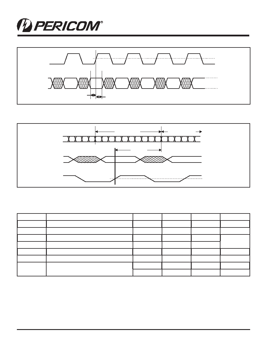
TX<9:0>
TX_CLK
tHOLD
tSETUP
1.4V
2.0V
0.8V
DATA
Figure 3. Transmitter Section Timing
T5 T6 T7 T8 T9 T0 T1 T2 T3 T4 T5 T6 T7 T8 T9 T0 T1 T2 T3 T4 T5
DATA BYTE A
DATA BYTE B
DATA BYTE C
1.4V
DOUT±
TX<9:0>
TX_CLK
t_TXLAT
Figure 4. Transmitter Latency
Notes:
1.
This is the recovery for input phase jumps.
2.
The receiver latency as shown in Figure 6, is dened as the time between receiving the rst serial bit of a parallel data word (dened as the
rst edge of the rst serial bit) and the clocking out of that parallel word (dened by the rising edge of the receive byte clock, either RBC1 or
RBC0).
09-0001
相關(guān)PDF資料 |
PDF描述 |
|---|---|
| PIC10F206-I/P | IC PIC MCU FLASH 512X12 8DIP |
| PIC10F222-E/OT | IC PIC MCU FLASH 512X12 SOT-23-6 |
| PIC10F222-I/P | IC PIC MCU FLASH 512X12 8DIP |
| PIC10LF322T-I/OT | MCU 8BIT 896B FLASH SOT23-6 |
| PIC12C508-04I/SM | IC MCU OTP 512X12 8-SOIJ |
相關(guān)代理商/技術(shù)參數(shù) |
參數(shù)描述 |
|---|---|
| PI90SD1636CFD | 制造商:PERICOM 制造商全稱:Pericom Semiconductor Corporation 功能描述:SERDES Gigabit Ethernet Transceiver |
| PI90SD1636CFDE | 制造商:PERICOM 制造商全稱:Pericom Semiconductor Corporation 功能描述:SERDES Gigabit Ethernet Transceiver |
| PI90SD1636DFCE | 功能描述:以太網(wǎng) IC 1.25Gbaud Gigabit Ethernet RoHS:否 制造商:Micrel 產(chǎn)品:Ethernet Switches 收發(fā)器數(shù)量:2 數(shù)據(jù)速率:10 Mb/s, 100 Mb/s 電源電壓-最大:1.25 V, 3.45 V 電源電壓-最小:1.15 V, 3.15 V 最大工作溫度:+ 85 C 封裝 / 箱體:QFN-64 封裝:Tray |
| PI90SD1636DFCEX | 功能描述:以太網(wǎng) IC 1.25Gbaud Gigabit Ethernet RoHS:否 制造商:Micrel 產(chǎn)品:Ethernet Switches 收發(fā)器數(shù)量:2 數(shù)據(jù)速率:10 Mb/s, 100 Mb/s 電源電壓-最大:1.25 V, 3.45 V 電源電壓-最小:1.15 V, 3.15 V 最大工作溫度:+ 85 C 封裝 / 箱體:QFN-64 封裝:Tray |
| PI96B30P00F00Z1 | 功能描述:DIN 41612 連接器 DIN MALE 96 POSITIO RoHS:否 制造商:HARTING 系列:har-bus 64 產(chǎn)品類型:Plugs 排數(shù):5 位置/觸點數(shù)量:160 安裝角:Right 類型:Shrouded Header 端接類型:Solder 外殼材料: 觸點材料: 觸點電鍍: |
發(fā)布緊急采購,3分鐘左右您將得到回復(fù)。